According to Reuters, Intel’s ambitions to become the world’s second-largest contract chipmaker by 2030 seem to have encountered a major hurdle after Broadcom’s trial runs using Intel’s 18A fabrication technology did not purportedly meet expectations. This setback adds pressure to Intel’s revival plan and a goal to leave TSMC behind in manufacturing process advancements, but the situation is not that dramatic.
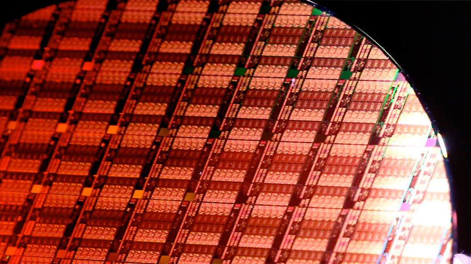
To test Intel’s 18A (1.8nm-class) process technology, Broadcom produced wafers with test patterns typical of the products it designs. After the company received these shuttle wafers, its engineers and executives were allegedly unsatisfied with the production node, claiming it was ‘not yet viable to move to high-volume production,’ according to Reuters' sources. It could be a blow for Intel’s foundry unit, but Intel disclosed defect density for its 18A process last week, and it looks healthy enough for a node that will enter mass production two or three quarters down the road.
“I am happy to update the audience that that we are now, for this production process, we are now below 0.4 d0 defect density, this is now a healthy process,” said Pat Gelsinger, chief executive of Intel, at the Deutsche Bank’s 2024 Technology Conference.
Generally, it is considered that a defect density below 0.5 defects per square centimeter is a good result, so even keeping in mind that defect density varies by process and application, Intel 18A’s defect density of 0.4 defects per square centimeter is a reasonably good result considering its timing. Yet, TSMC’s N7 and N5 technologies had a defect density of 0.33 at a similar development stage, and when TSMC’s N5 reached mass production, its defect density dropped to 0.1. Yet, TSMC’s N3 started with a higher defect density but matched N5’s defect rate after five to six quarters.
Also, Broadcom has yet to finalize its assessment of Intel’s 18A manufacturing technology, signaling that its evaluation is ongoing, the company’s spokesperson told Reuters.
Broadcom is a major supplier of chips for telecommunication equipment as well as one of the world’s leading contract chip designers, which develops TPU AI processors for Google and is rumored to be working on AI processors for OpenAI, which makes Broadcom a particularly important customer for TSMC and a desired client for other foundries, including Intel. But it takes a lot to serve Broadcom properly.
Earlier this year, Broadcom demonstrated what was considered the world’s largest processor at the time. The XPU used two near the reticle limit (858mm^2, 26 mm by 33 mm) to compute chiplets with six HBM3 memory stacks each (i.e., 12 HBM3 stacks total). In context, Nvidia’s B200 GPU consists of two near-reticle limits compute chiplets and eight HBM3E stacks.
Creating a chiplet of this size is a significant achievement. Achieving a good yield with such a chiplet is another milestone, and Broadcom’s and Nvidia’s foundry partner TSMC has succeeded in this. It means that to serve Broadcom using its 18A process technology, Intel needs to be able to make chaplets of this scale with good yields, which is not easy. Whether or not the company will be able to meet Broadcom’s requirements for defects and yields of big chips with its 18A in 2025 remains to be seen, but for now, Broadcom does not seem to be satisfied.


