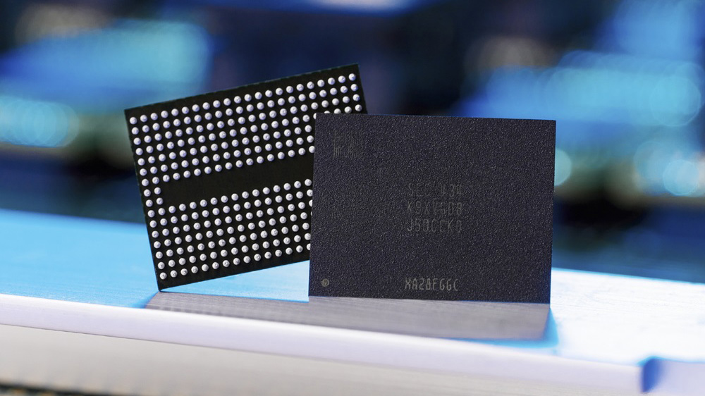
After launching its new V9 TLC NAND flash in April, Samsung announced the initial mass production of its bleeding-edge 9th-generation V9 QLC flash memory. The more storage-spacious V9 flavor is being mass-produced in one-terabit models.
Samsung revealed that its V9 QLC flash takes advantage of Channel Hole Etching technology to achieve the highest layer counts in the industry, featuring a double-stack design. Using lessons learned from its 9th-gen TLC variant, V9 QLC is approximately 86% denser than the previous generation of QLC V-NAND flash. Samsung also uses Designed Mold technology and Predictive Program technology to boost data retention performance by roughly 20% and data input/output speed by 60%.
The company has also reduced power consumption massively thanks to a feature Samsung calls Low-Power Design. This technique reduces the voltage that drives the NAND cells by sending only the necessary bit lines, reducing power consumption by 30% and 50% respectively for the data reads and writes.
Samsung plans to expand its 9th-gen QLC into various products, from mainstream SSDs to mobile smartphone UFS storage. Samsung also specifically states that QLC will be available to its cloud service provider customers as server-based SSDs.
We first saw reports of V9 QLC nine months ago. Samsung's new 280-layer QLC is purportedly the best in the industry, boasting by far the best density and performance compared to its competitors' best QLC solutions. Storage density is 19.5 Gb mm2, making V9 almost 50% denser than the next best solution, YMTC's 20.63mm2 232-layer QLC. Performance is purportedly 33% faster than its competitors, with an operating speed of 3.2 Gbps.
With these enhancements, Samsung will be able to make drives nearly 50% cheaper than the highest-capacity SSDs on the market today, whether that be consumer PCIe M.2 SSDs, server U.2 SSDs, or large-form-factor SSDs. The performance will also be substantially better, with V9 QLC possibly performing close to older/budget SSDs using TLC NAND flash.


