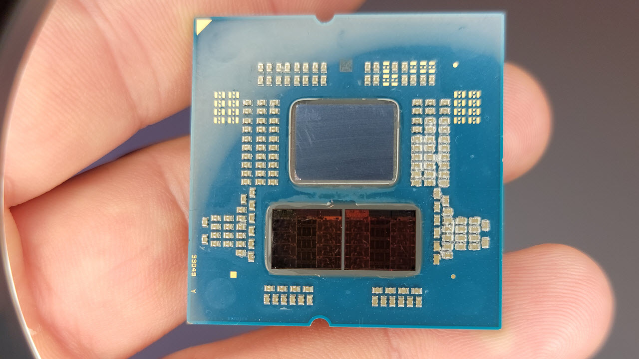
AMD revealed the deep-dive details of its Zen 5 Ryzen 9000 ‘Granite Ridge’ and Ryzen AI 300 series ‘Strix Point’ chips at its Zen 5 Tech Day, digging into the company’s next-generation silicon that will vie for a spot on our list of best CPUs for gaming. AMD has slowly teased the details of its Zen 5 processor, but today, we can share more in-depth AMD benchmarks of desktop and mobile Ryzen processors against competing Intel, Apple, and Qualcomm processors.
AMD also unveiled a new series of motherboards and gave deep dives into the Zen 5 CPU, RDNA 3.5 GPU, and XDNA 2 NPU microarchitectures. We’ll cover these in full on the following pages as AMD speeds toward an on-time launch of its desktop and mobile processors this month.
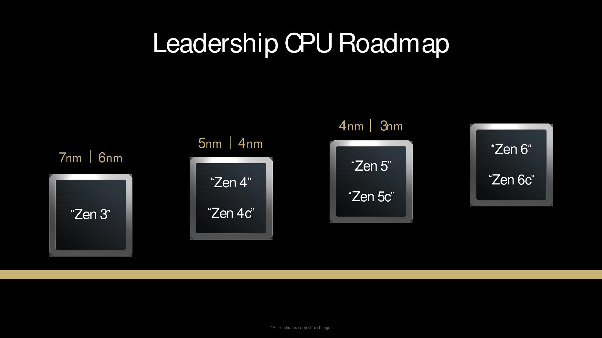
AMD’s Zen 5-powered chips come to market bearing a new microarchitecture bristling with improvements that yield an average 16% increase in instructions per cycle (IPC) throughput. As you can see in the roadmap above, the Zen 5 architecture will span both the 4nm (N4P) and 3nm process nodes over the course of its life. This means that, much like the company’s other generations of microarchitectures, we can expect second-gen models with even more performance to arrive on a smaller process node. Let’s dive into the details of the processors and benchmarks, then move on to the architectures.
AMD Zen 5 Ryzen 9000 ‘Granite Ridge’ Benchmarks and Specs
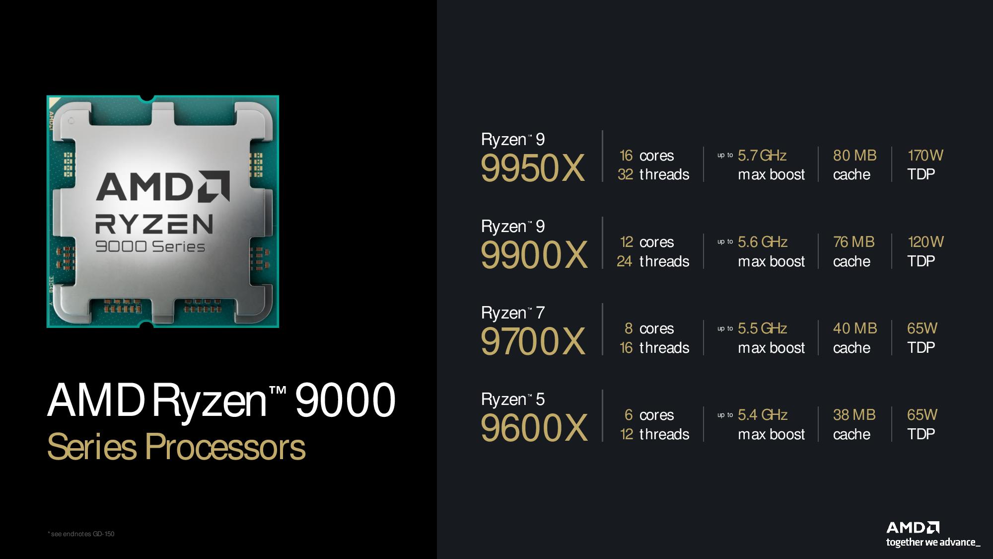
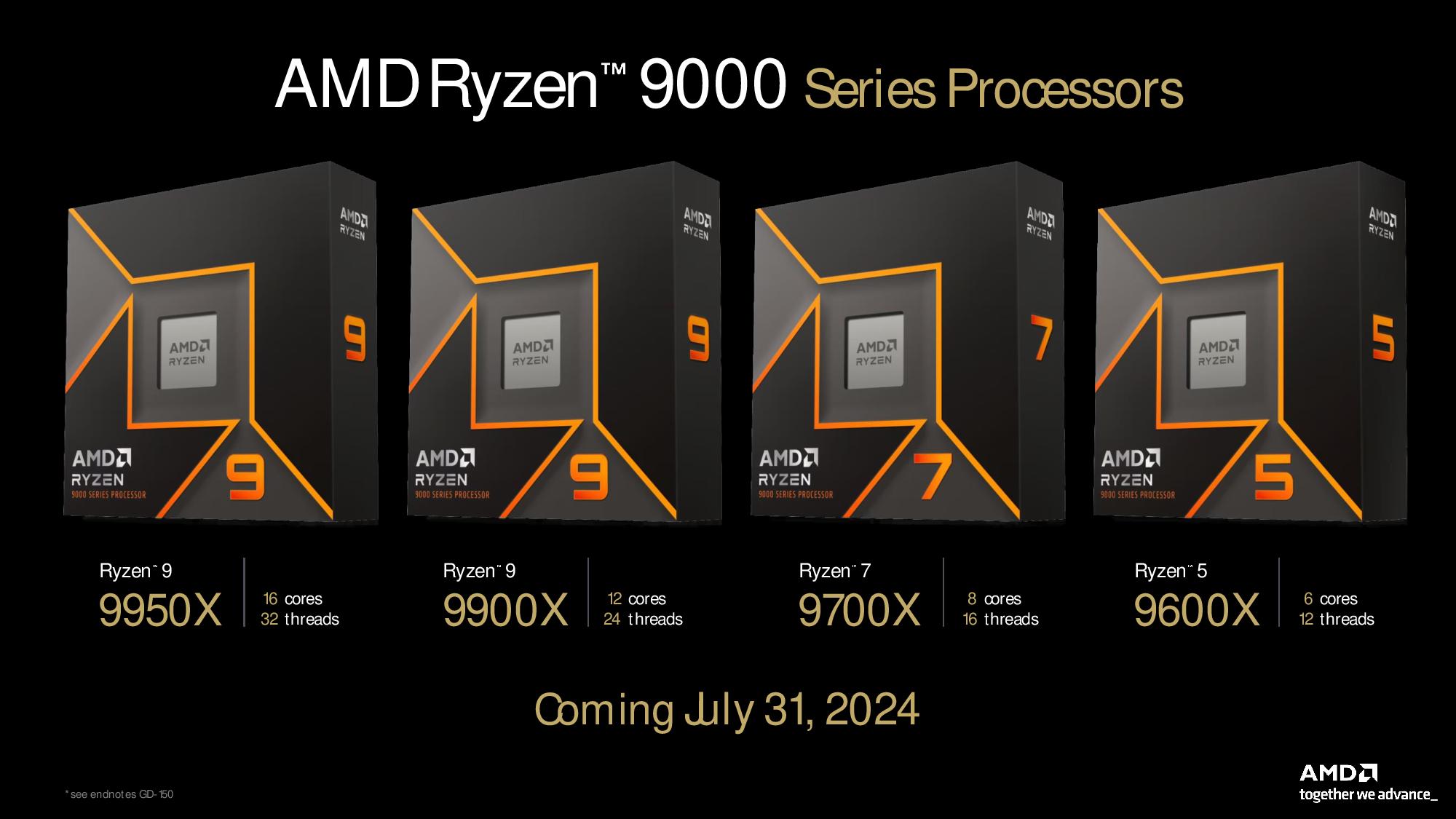
We’ve already covered the Ryzen 9000 series product stack, which you can see here. As a reminder, all models except the flagship have lower TDPs than their predecessors yet still deliver impressive generational performance gains. AMD still hasn’t shared pricing, but we’re told an announcement will come before Ryzen 9000’s July 31 launch date.
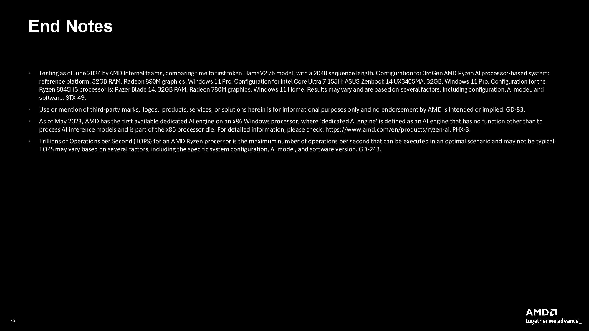
All the Ryzen 9000 models drop into existing AM5 platforms and also support the upcoming 800-series chipset family, which we’ll cover below. As such, these chips support many of the same features as before, including PCIe 5.0 and DDR5-5600 memory. As with all vendor-provided benchmarks, take these with a grain of salt (test notes at the end of the album).
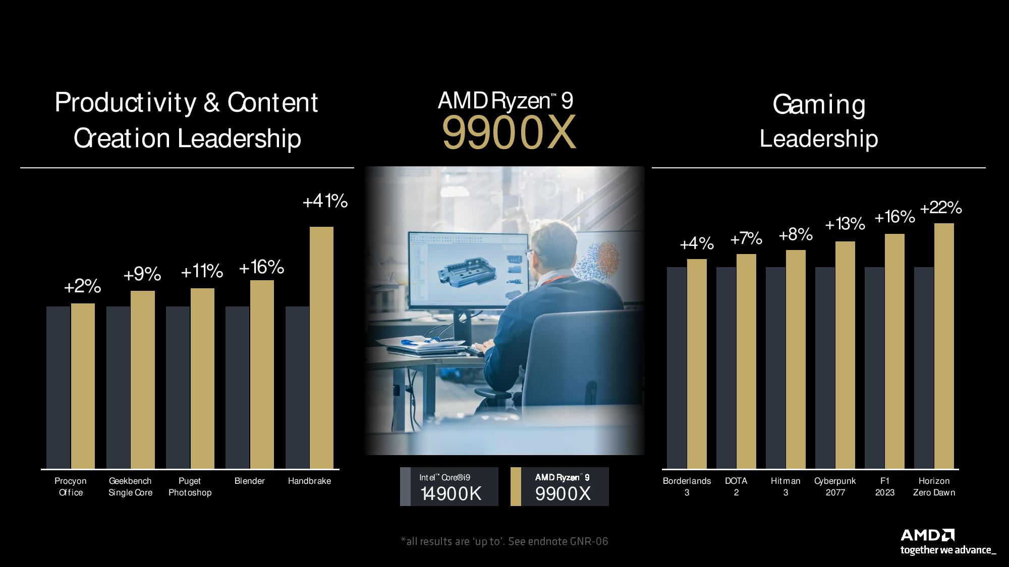
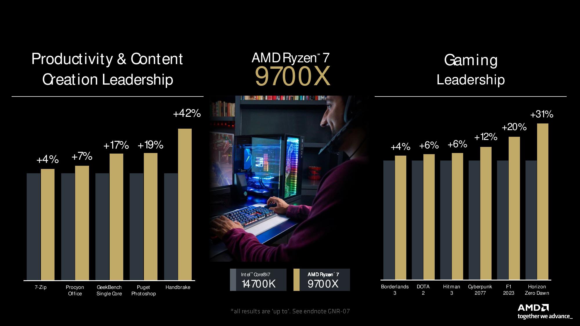
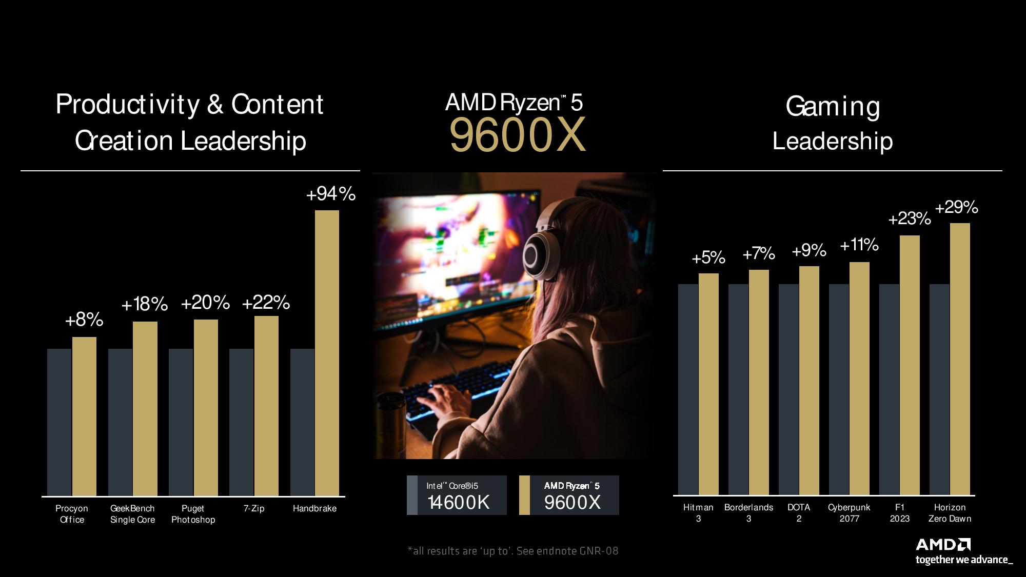
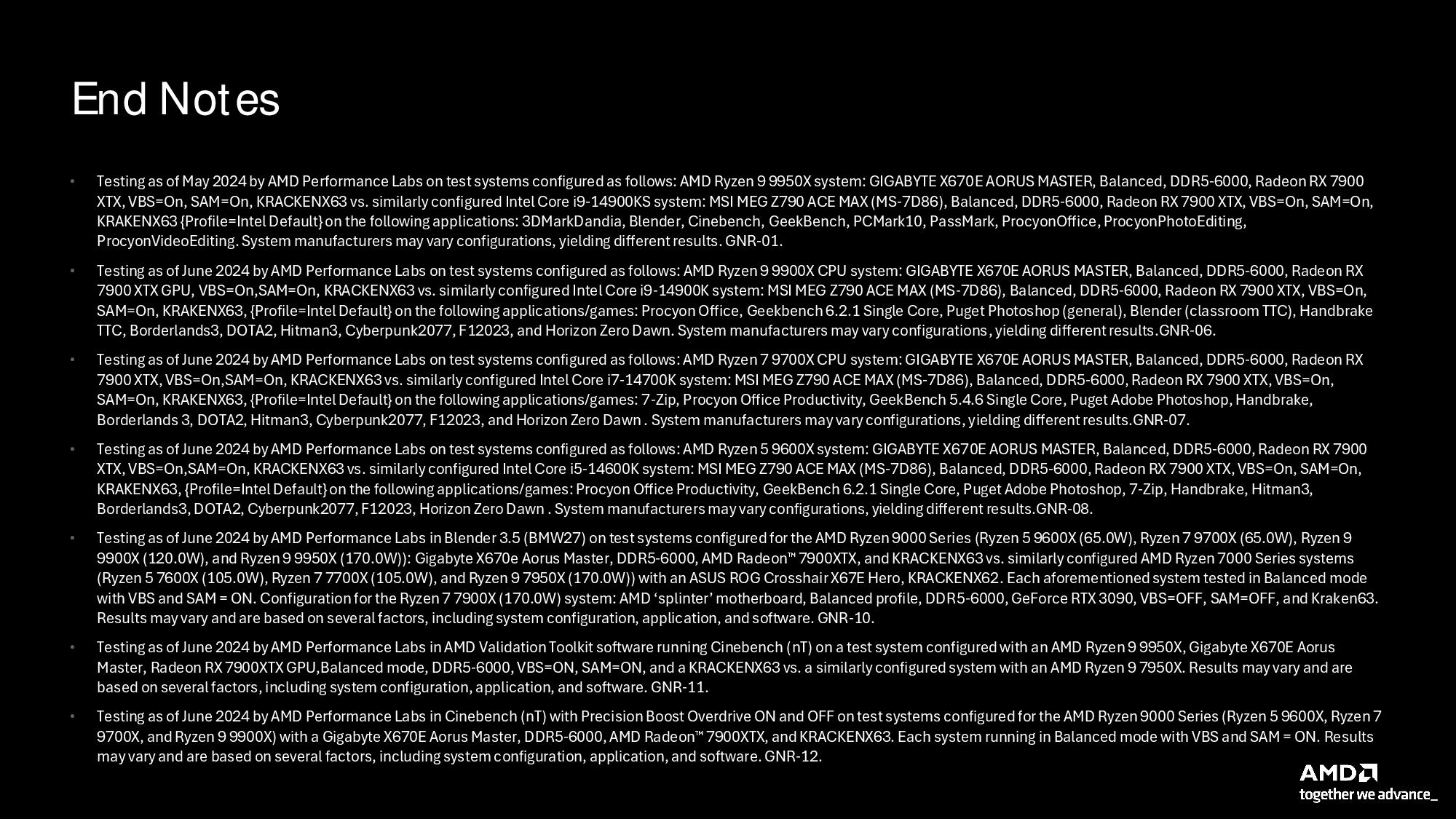
AMD has previously shared benchmarks showing the flagship 16-core 32-thread Ryzen 9 9950X against Intel’s Core 9-14900K with an average of a 21% advantage in productivity and 11% in gaming. Notably, a portion of the productivity gains come from Ryzen 9000’s doubled performance in AVX-512 workloads, but the uplift in other types of workloads is also impressive across the board.
AMD’s 12-core 24-thread Ryzen 9 9900X is equally impressive in its comparison with the 14900K, notching anywhere from a 2% to 41% lead in a range of productivity applications. It also takes from a 4% to 22% lead over the 14900K in a range of game titles. All told, these figures work out to a ~10% lead in both productivity and gaming over Intel’s flagship (geomean).
The Ryzen 9 9900X’s win is particularly noteworthy given that this 120/162W chip (a 68W reduction in peak from prior gen) faces a 125/253W Intel chip known for easily reaching 350W with power limits removed. Of course, Intel’s Arrow Lake chips will arrive later this year to challenge this power/performance lead.
The eight-core 16-thread Ryzen 7 9700X faces off with the Core i7-14700K in the benchmarks. AMD’s advantage in productivity work becomes more significant despite the fact we’re again looking at a power-sipping AMD 65/88W chip versus a 125/253W Intel model. Overall, AMD claims a ~13% lead in productivity apps and a 10% lead in gaming.
The six-core 12-thread Ryzen 5 9600X contends with the Core i5-14600K (88W vs 181W peak power draw, respectively) and takes a 22% lead in productivity performance (15% without HandBrake outlier) and an 11% lead in gaming. That represents a strong performance gain at the bottom of the Zen 5 CPU stack.
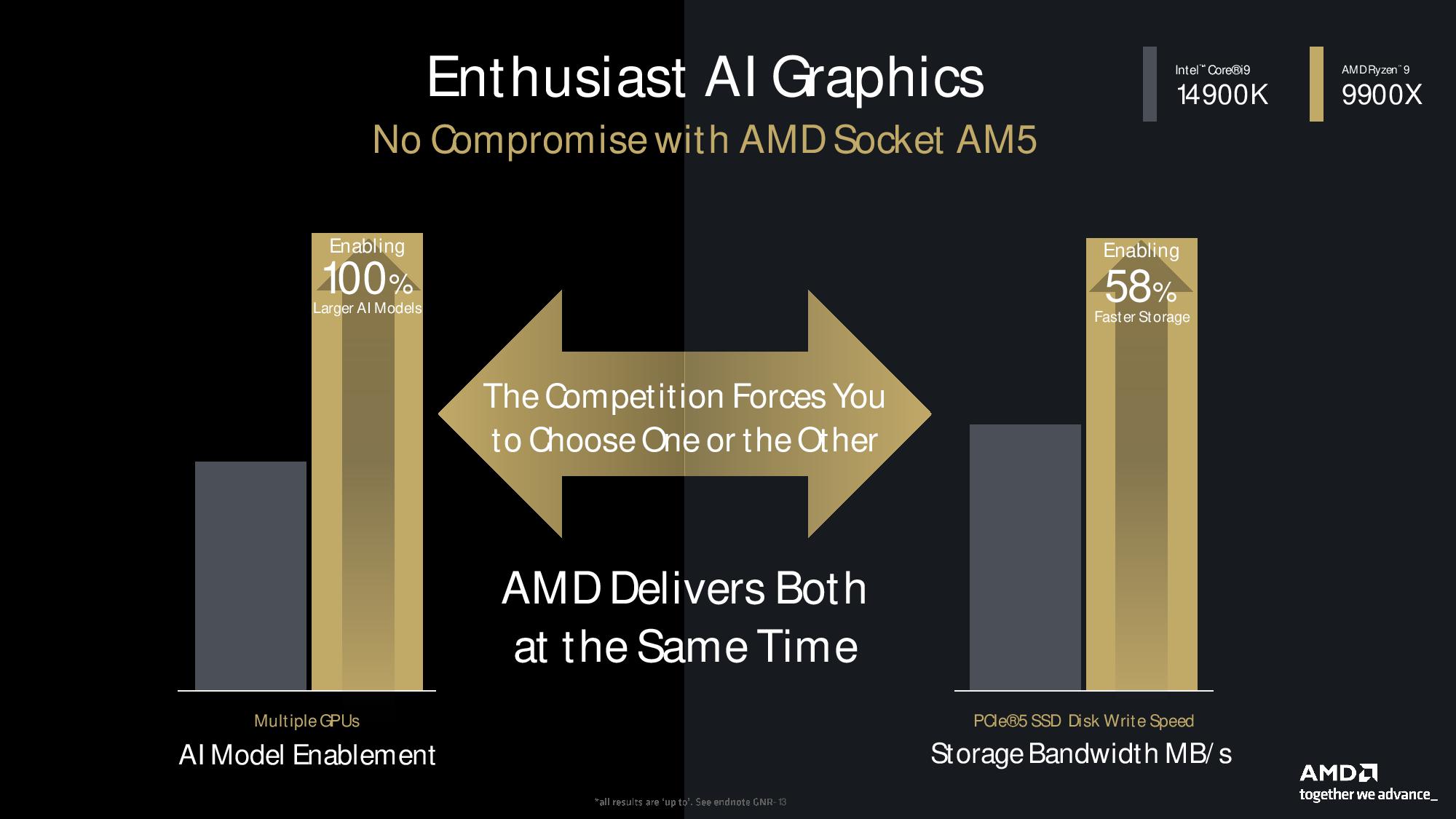
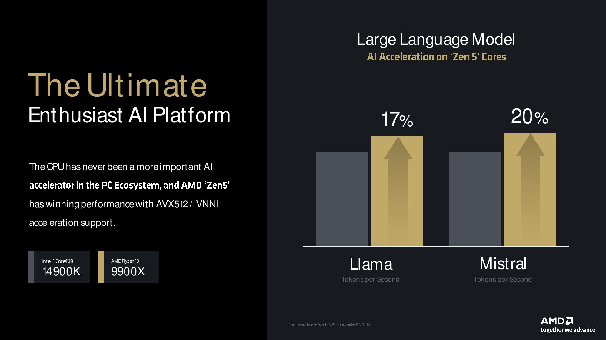
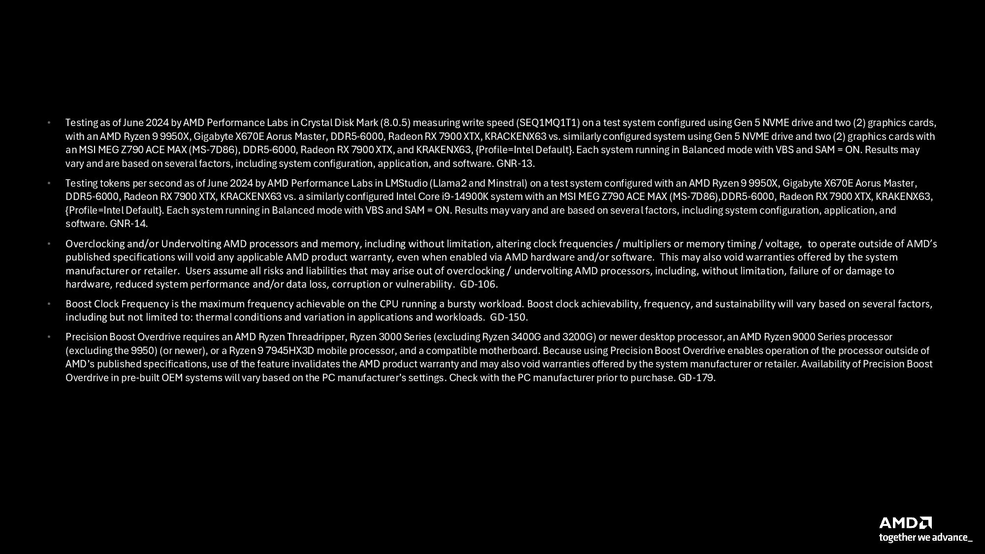
AMD also included AI benchmarks that highlight the advantages of its support for VNNI (an AI-optimized instruction set) for running the Llama and Mistral Large Language Models (LLMs) on Zen 5 processors. As you can see, the Ryzen 9 9900X easily beats the 14900K, but we don’t think this is a very pertinent comparison — most would simply run these models on a GPU. AMD also showcased its PCIe lane advantage over Intel’s current chips, which results in more performance when running an AI model on multiple GPUs while maintaining the full PCIe 5.0 speed for the attached SSD. AMD wins in these AI workloads, but again we don’t see these as relevant workloads for the majority of desktop PC users.
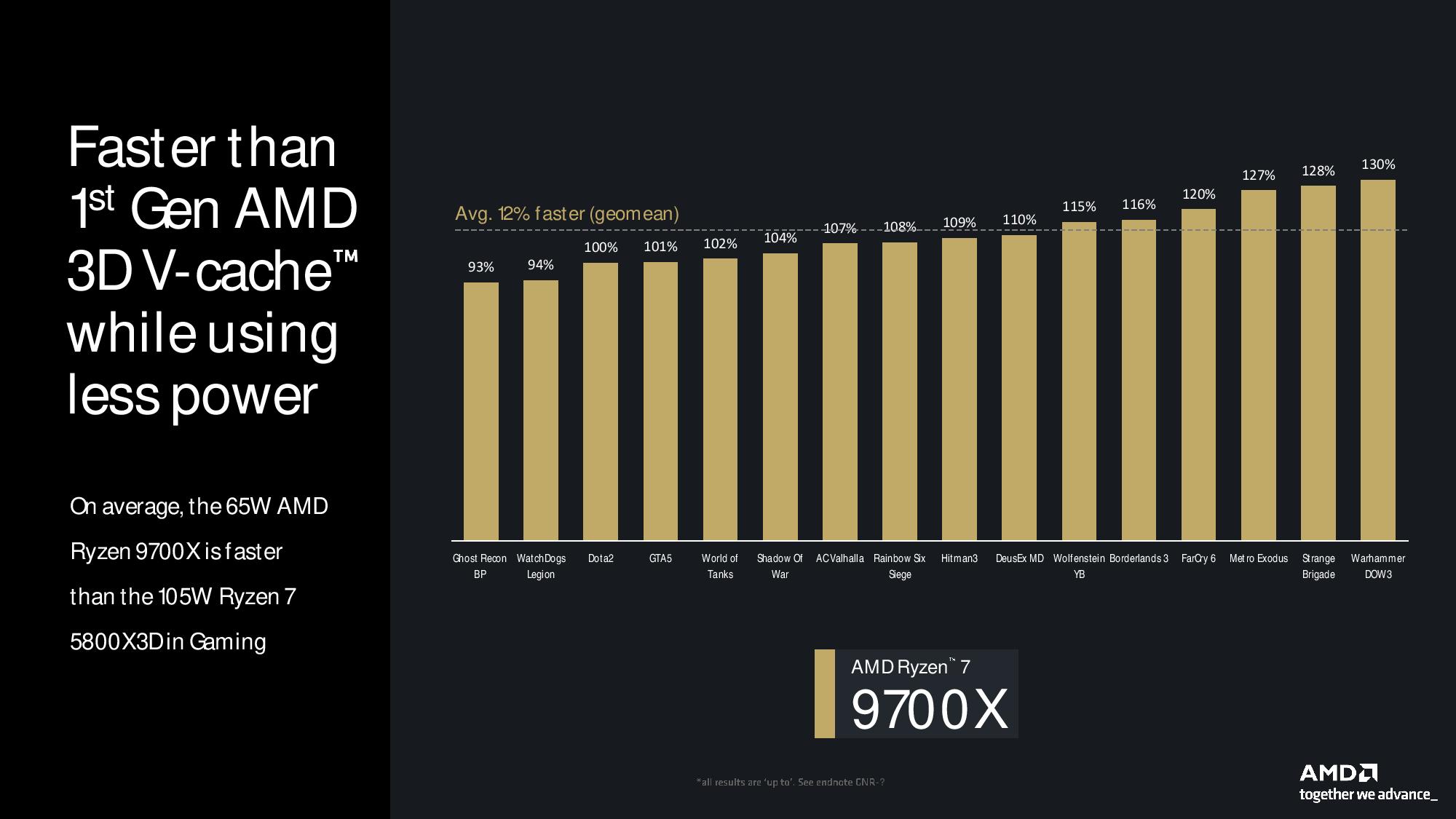
AMD underscored Zen 5’s leap forward in gaming performance by comparing the 9700X to the fastest Zen 3 gaming chip, the Ryzen 7 5800X3D. Long after its release for the AM4 platform, the Zen 3-powered 5800X3D has maintained a significant lead over AMD’s newer standard Zen 4 processors — to this day, it beats the fastest standard Zen 4 chip by roughly 8% in gaming. Now, you’d have to step up to a pricier Zen 5 X3D model to beat the 5800X3D in gaming, but AMD claims Zen 5 Ryzen 7 9700X is roughly 12% faster in 1080p gaming than the 5800X3D, despite its 40W lower power draw.
Notably, AMD avoided comparing its new chips to its own previous-gen Zen 4 models but says the 9700X would beat the Ryzen 7 7800X3D, currently the best gaming CPU on the market, by a “couple percentage points.” These results imply the Ryzen 7 9700X delivers a roughly ~20% gain in gaming performance over the previous-gen Ryzen 7 7700X.
The individual gaming results still warrant a look as well. There remain a few games in AMD's tests where the 9700X failed to beat the 5800X3D, never mind the newer 7800X3D. For those games that really like the large L3 cache, the IPC and other improvements still won't close the gap and we'll need to wait for the inevitable Zen 5 X3D parts to arrive later this year.
The TSMC N4P node and Zen 5 IPC
AMD’s engineers confirmed our suspicion that the Zen 5 processors use TSMC’s N4P node, a marked improvement over Zen 4’s 5nm node. This is important because TSMC’s standard 4nm node (N4) offers much less of an improvement over 5nm, whereas N4P delivers the some of the best generational improvements of the 4nm lineup (TSMC’s 4nm node is officially part of its 5nm family).
TSMC says the N4P node offers 11% more performance, 22% higher power efficiency, and 6% higher transistor density (optical shrink) than the N5 (5nm) node. Additionally, TSMC says this process uses 6% fewer masks for production due to an increased number of EUV layers, implying that it’s more cost-effective. AMD has also designed the Zen 5 process for the TSMC 3nm node, but the company hasn’t given any details on the node or the launch date for those chips.
The N4P process node obviously helps deliver faster and more power-efficient processor performance. Paired with the 16% increase in IPC, AMD's Zen 5 is exceptionally promising. We'll dive deeper into the IPC gain on the Zen 5 architecture page. First, let's take a look at power efficiency, overclocking, motherboards, and Ryzen AI 300.
Zen 5 Ryzen 9000 Power Efficiency and Thermals
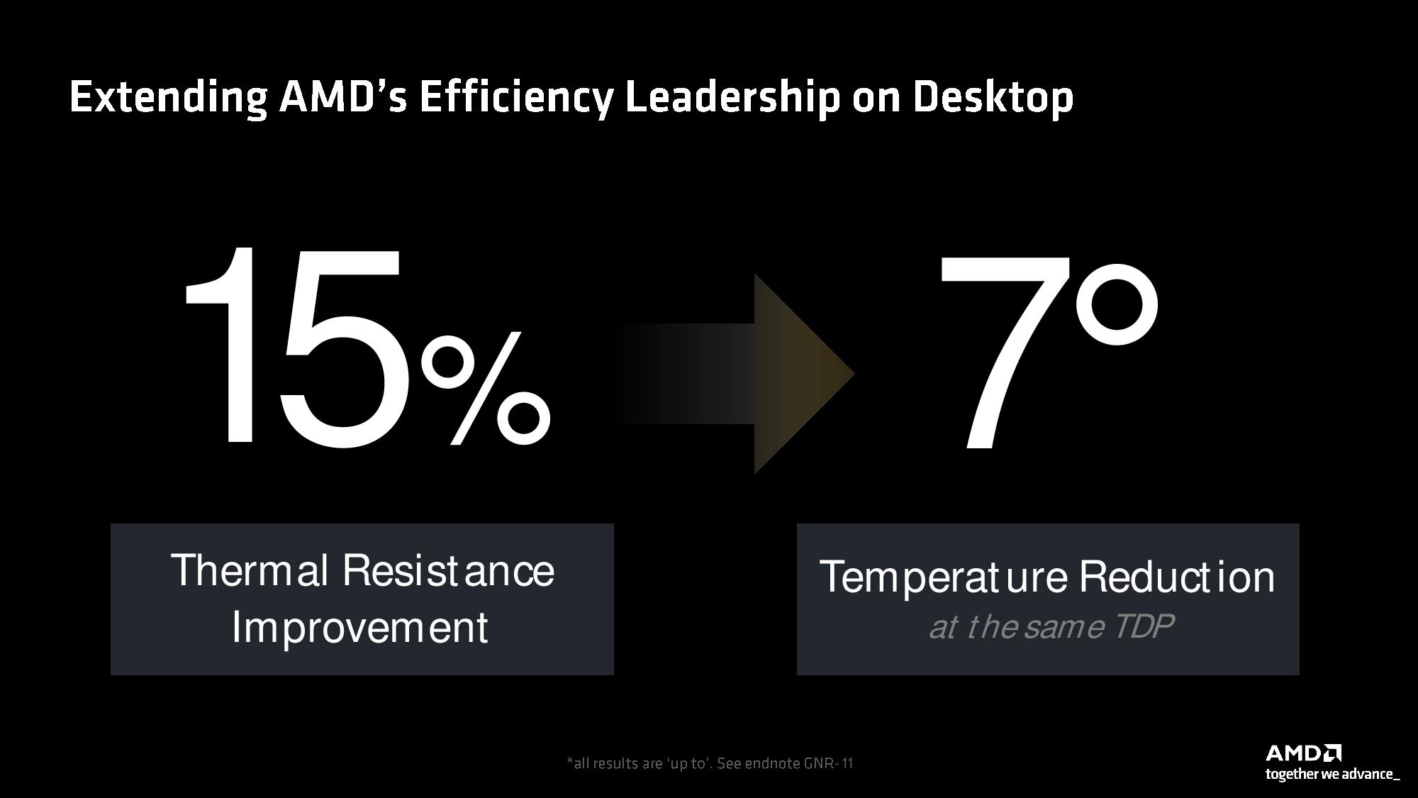
AMD says Ryzen 9000 series runs at much lower temperatures than its predecessors, helping keep frequency residency high (better effective frequency and longer boost durations). This is due to a 15% improvement in thermal resistance, which allows the chip to operate at a 7C lower temperature than a Zen 4 chip running at the same TDP.
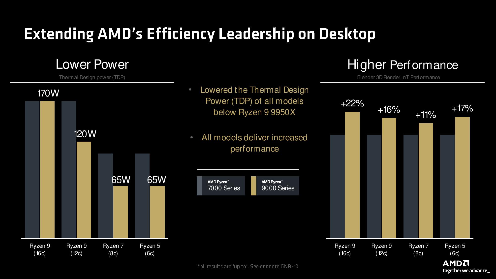
As you can see in the second slide above, Ryzen 9000’s improved thermal performance allowed dialing back the TDP for three of the four new desktop chips, all while delivering substantial performance improvements in the types of heavy multi-threaded workloads that push the chip to its power limits. AMD used the Blender benchmark to highlight the improved performance in heavy workloads.
Some of the power improvements undoubtedly result from moving from the 5nm node to N4P, but AMD also made other targeted optimizations to wring out more performance. AMD’s engineers said hotspots were a challenge with the Zen 4 design, so they reduced the number of hotspots and better dispersed the remaining hot spots on the compute die. The engineers also fixed Zen 4’s ‘suboptimal’ placement of the temperature sensors spread across the die. Paired with a more intelligent firmware control algorithm, the better placement of the thermal sensors enables more accurate decisions for tighter control of the available temperature margin.
AMD says the result is a pronounced reduction in power usage that allows the system to run cooler and, ultimately, quieter than the previous-gen models, not to mention Intel's competing Raptor Lake Refresh.
New 800 Series Chipsets and Overclocking
AMD’s original AM4 platform is legendary for its longevity, supporting all versions of Ryzen since the lineup’s debut in 2017 (and even the Bristol Ridge series before). It now encompasses 145 CPU and APU models — and that list continues to grow.
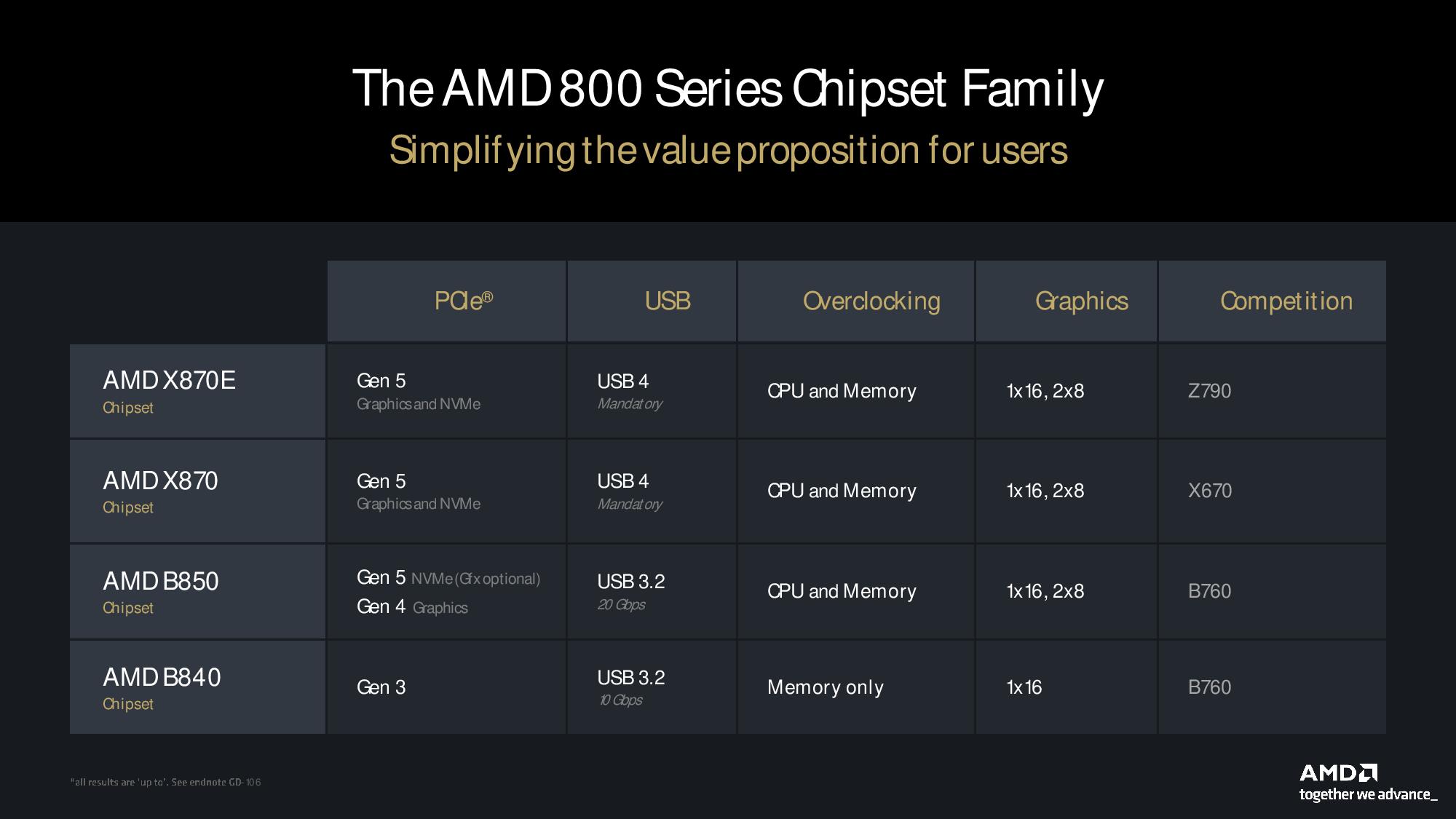
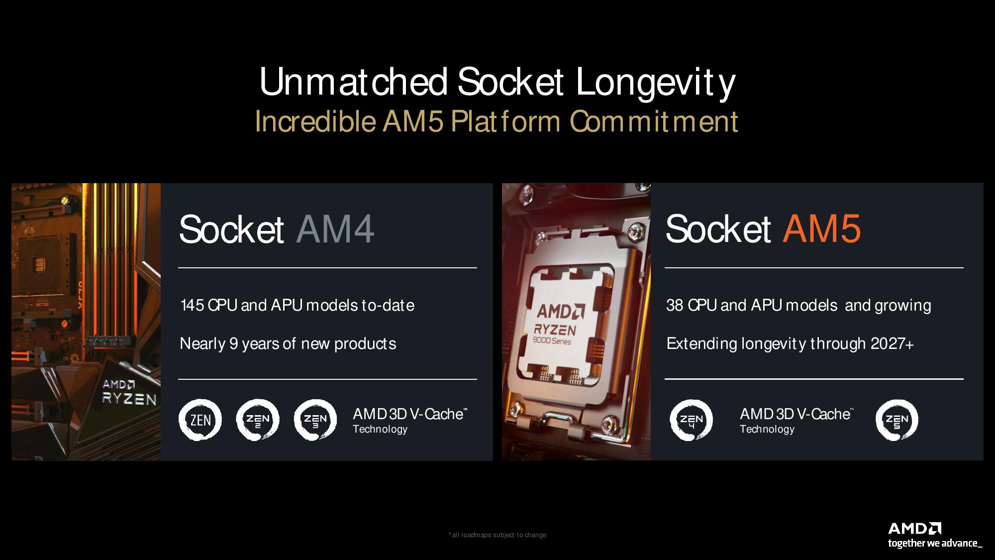
AMD says we can expect AM5 to last through 2027+, as it's also engineered for the long run. AMD already unveiled its top-tier X870 and X870E chipsets at Computex 2024, with the most notable additions being the mandatory addition of USB4 and PCIe 5.0 for both graphics and storage.
AMD is now announcing the value-oriented B-series chipset with a new tier in addition to the standard B850 we’d expect. The new B840 motherboards land between the bargain-basement A-series motherboards and the standard fully overclockable B850. There are several differences between the two tiers. B840 fully supports memory overclocking but does not support CPU overclocking like the higher-tier models. The B840 motherboards will also only have a PCIe 3.0 x16 connection — a big reduction from the PCIe 5.0 and 4.0 connections available on the B850 boards.
Both the B850 and B840 support USB 3.2 instead of the mandatory USB 4 present on the X-series motherboards. Even though AMD’s nagging AM5 pricing issues have largely receded, the B840 alterations create a less expensive B-series board that will provide more pricing flexibility, particularly for OEMs.
Unfortunately, AMD’s 800-series motherboards will not be available on the market when the Ryzen 9000 processors launch at the end of the month. AMD says that the various motherboard vendors will release on their own schedules, and our early indications are that the first motherboards will arrive at the end of September, well after the Ryzen 9000 launch date. The Ryzen 9000 chips are fully compatible with existing AM5 motherboards (after the requisite BIOS update), so there are options for early adopters. However, the staggered launch is obviously not ideal.
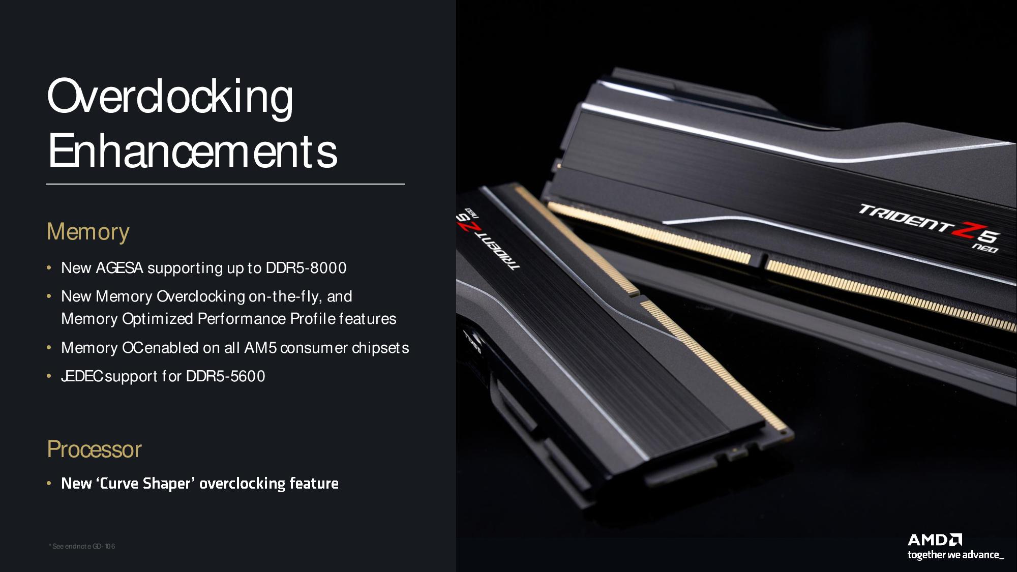
AMD has also made several enhancements on the overclocking front. The new 800-series AM5 boards will support higher memory overclocking ceilings than existing motherboards. AMD says the 800-series can support memory overclocking up to DDR5-8000. Ryzen 9000 also adds real-time memory overclocking, allowing you to change memory speeds and timings in real time from within the Ryzen Master application.
AMD also has a new Memory Optimized Performance Profile that allows either manual or automatic switching between the JEDEC and EXPO overclocking profiles in real time to prioritize either bandwidth or latency (timings) for the type of application that’s running. You can toggle between the different profiles in the Ryzen Master utility or enable automatic switching. The details behind this mechanism aren’t entirely clear yet, but we’ll learn more when the chips arrive for testing.
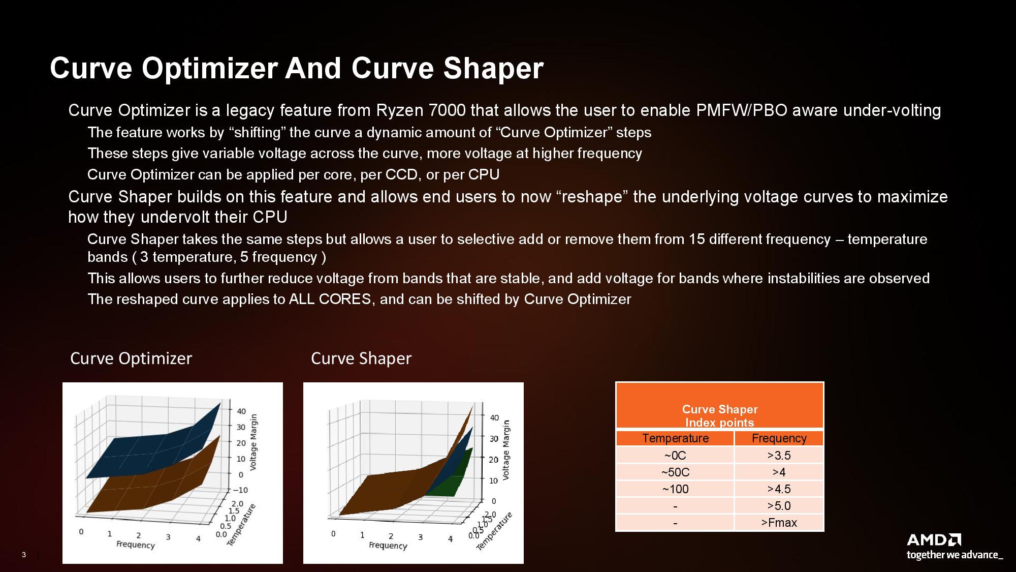
AMD’s existing Curve Optimizer feature allows you to set one negative or positive offset for the entire voltage/frequency curve, which the processor then applies across the full curve. The new Curve Shaper feature provides much more granular control by allowing adjustments for three temperature and five frequency points, resulting in 15 points of control for the user. That’s a major increase over the single point of control allowed with the existing mechanism.
AMD’s Ryzen Master already has an option for an automated test that can assign the Curve Optimizer offset. This will continue to work, but it will not offer the full 15 points of optimization — the Curve Shaper requires manual adjustment. However, the two features can be used in tandem, with the user assigning additional Curve Shaper points in addition to the single Curve Optimizer value (Curve Shaper acts as a sort of global modifier that will adjust all the assigned ranges).
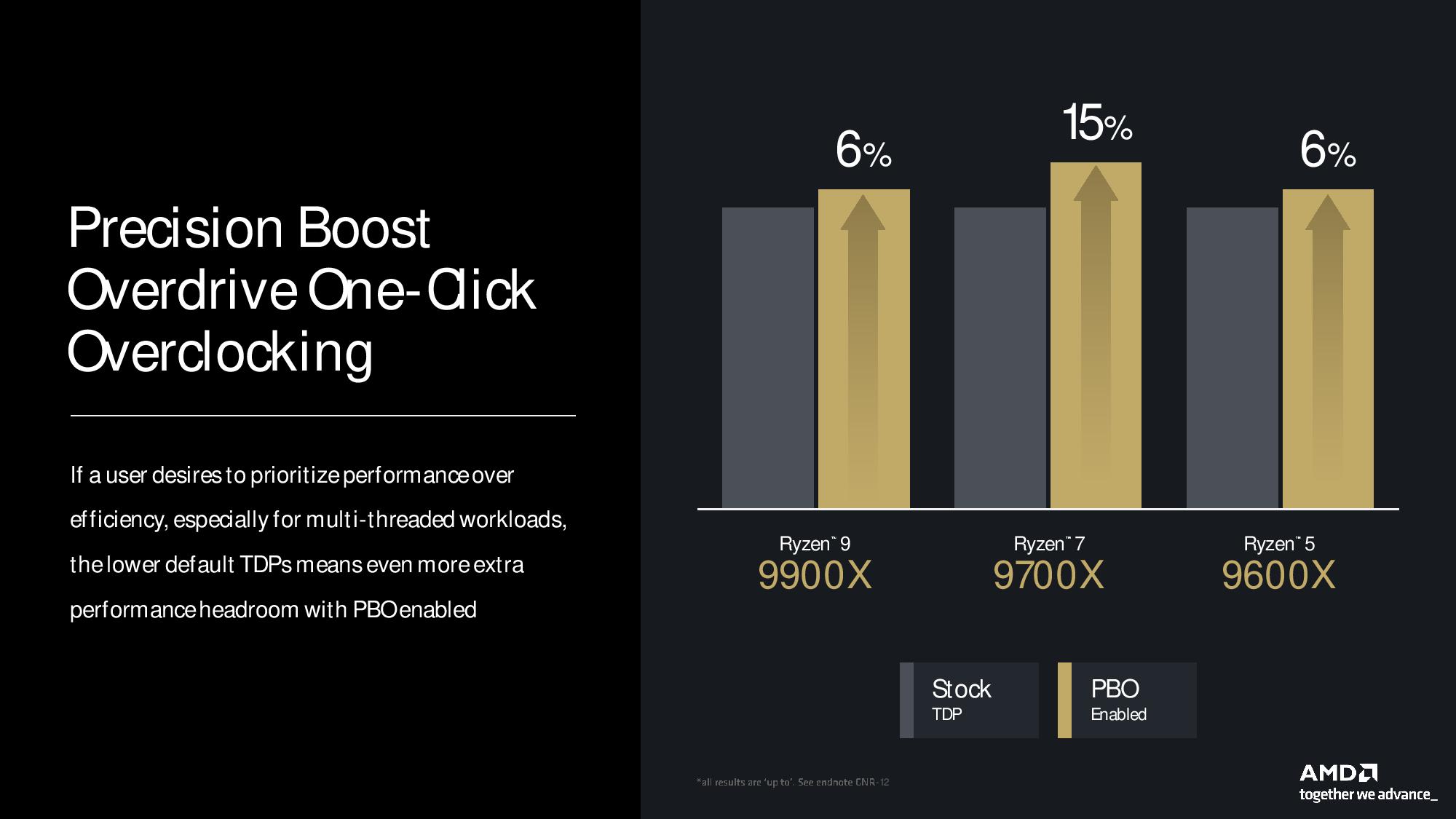
The auto-overclocking Precision Boost Overdrive (PBO) also returns, and AMD says Ryzen 9000’s lower TDP range enables more headroom for PBO gains. The company points to a 6% to 15% improvement in multi-threaded Cinebench performance with PBO engaged for the Ryzen 5, 7, and 9 processors but didn’t include the Ryzen 9 9950X in its PBO examples (likely a low single-digit percentage of gain). We’ll put all these new overclocking knobs to the test in our reviews.
On the following page, we will move on to the Ryzen AI 300 benchmarks and then on to the CPU, GPU, and NPU architectures.
AMD Zen 5 Ryzen AI 300 ‘Strix Point’ Gaming and Productivity Benchmarks
AMD also unveiled the Ryzen AI 300 ‘Strix Point’ processors at Computex 2024. The first laptops with the processors will be available this month at major retailers. AMD didn’t announce any new Strix Point chips but shared new benchmarks.
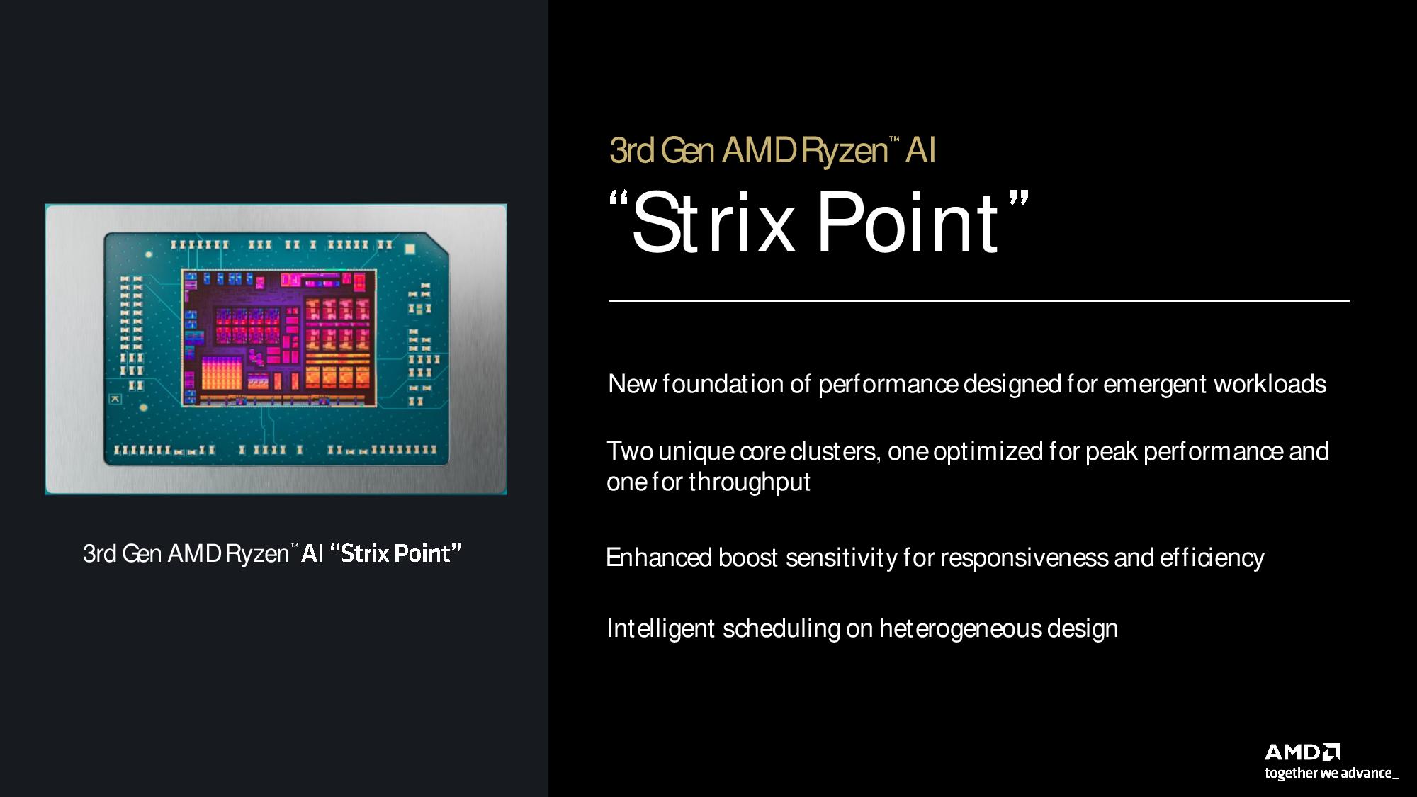
AMD will launch with the 12-core, 24-thread Ryzen AI 9 HX 370 (four Zen 5 cores and eight density-optimized Zen 5c cores) and the 10-core, 20-thread Ryzen AI 9 365 (four Zen 5, six Zen 5C).
The company’s benchmarks focused solely on the Ryzen AI 9 HX 370 in the Asus Zenbook S 16 compared to the Intel Core Ultra 9 185H in the Asus Vivobook S 16, and, of course, the elephant in the room: The Snapdragon X Elite X1E-84-100 in the Samsung Galaxy Book 4 (test notes are at the end of the album).
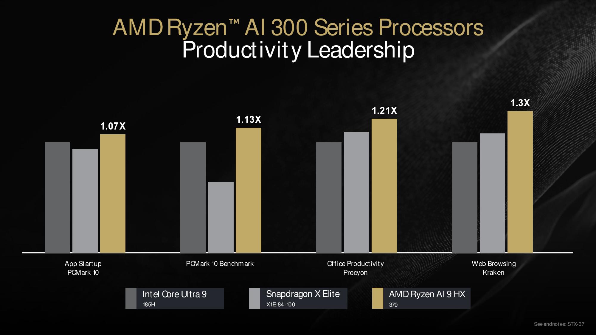
AMD’s productivity benchmarks show a 7% advantage in PCMark 10’s application startup test, a 13% lead in the full PCMark 10 benchmark, a 21% lead in the Procyon office productivity suite, and a 30% advantage in the Kraken web browsing JavaScript benchmark. However, these percentages appear to be relative to the Intel Core Ultra chip and not the Snapdragon laptop. The lack of a labeled axis makes comparisons to the X Elite difficult.
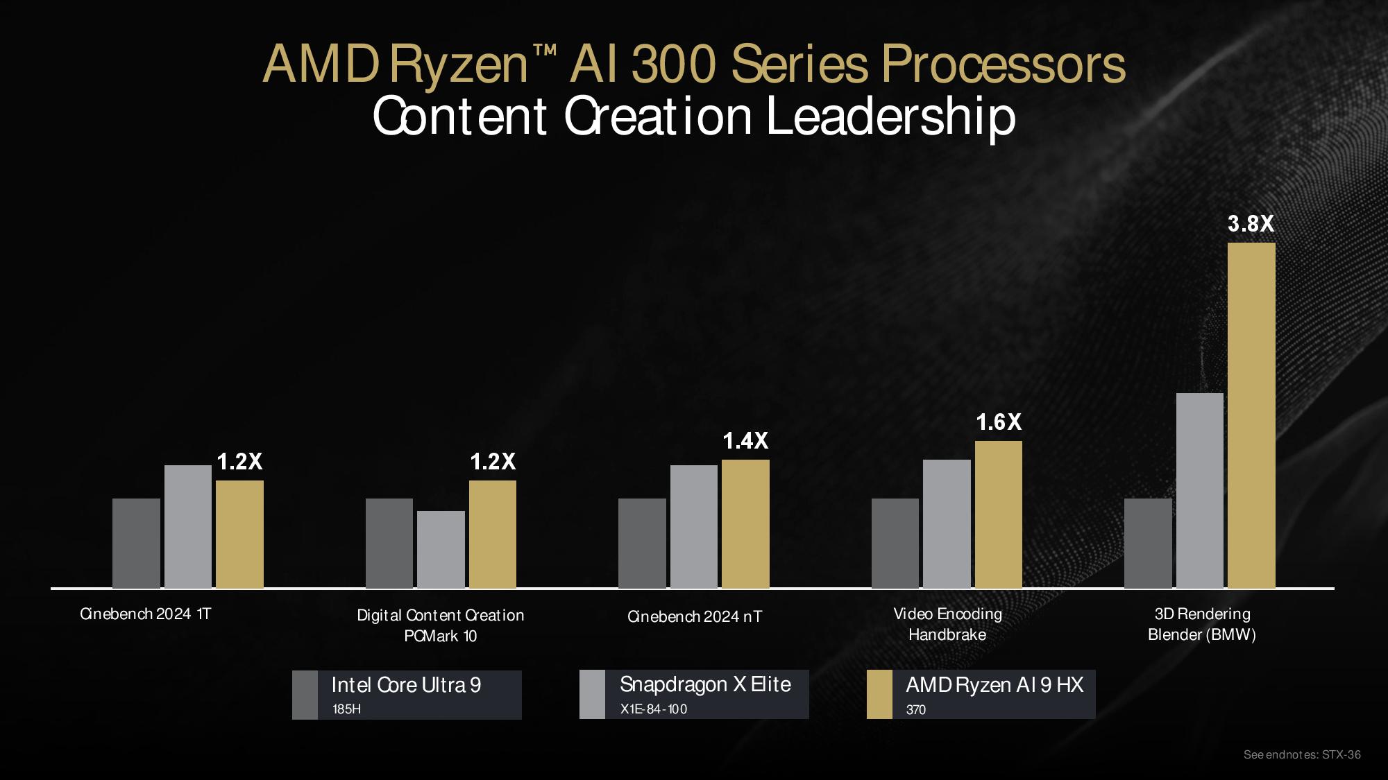
We see another round of somewhat hard-to-decipher results in the content creation tests, but the Ryzen processor takes the overall lead in all but the single-threaded Cinebench 2024 benchmark. There, the Snapdragon X Elite takes the lead, despite the 1.2X label on the AMD chip, and the X Elite is also within striking distance in the multi-threaded Cinebench benchmark. AMD enjoys a massive advantage in the Blender benchmark and carves out respectable leads in HandBrake and PCMark 10, too.
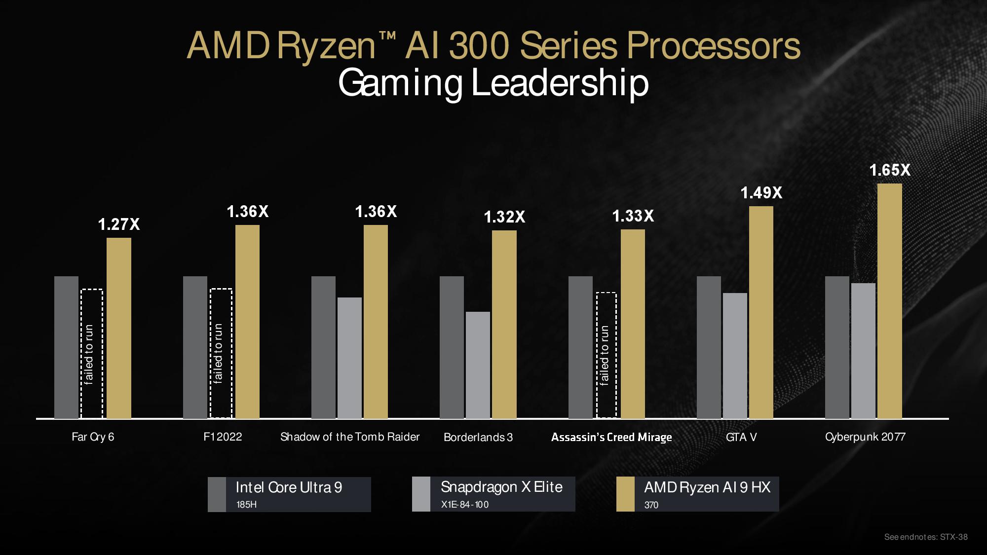
AMD also took on its competitors in gaming, claiming anywhere from a 27% to 65% lead over the Intel Core Ultra 9 processor. Still, again, the specific advantages over the X Elite are less discernible due to poor chart labeling. AMD is however quick to point out that three of the game titles failed to run on the X Elite processor, which isn’t entirely surprising.
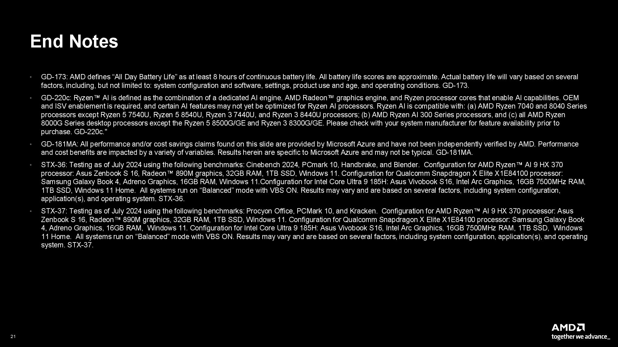
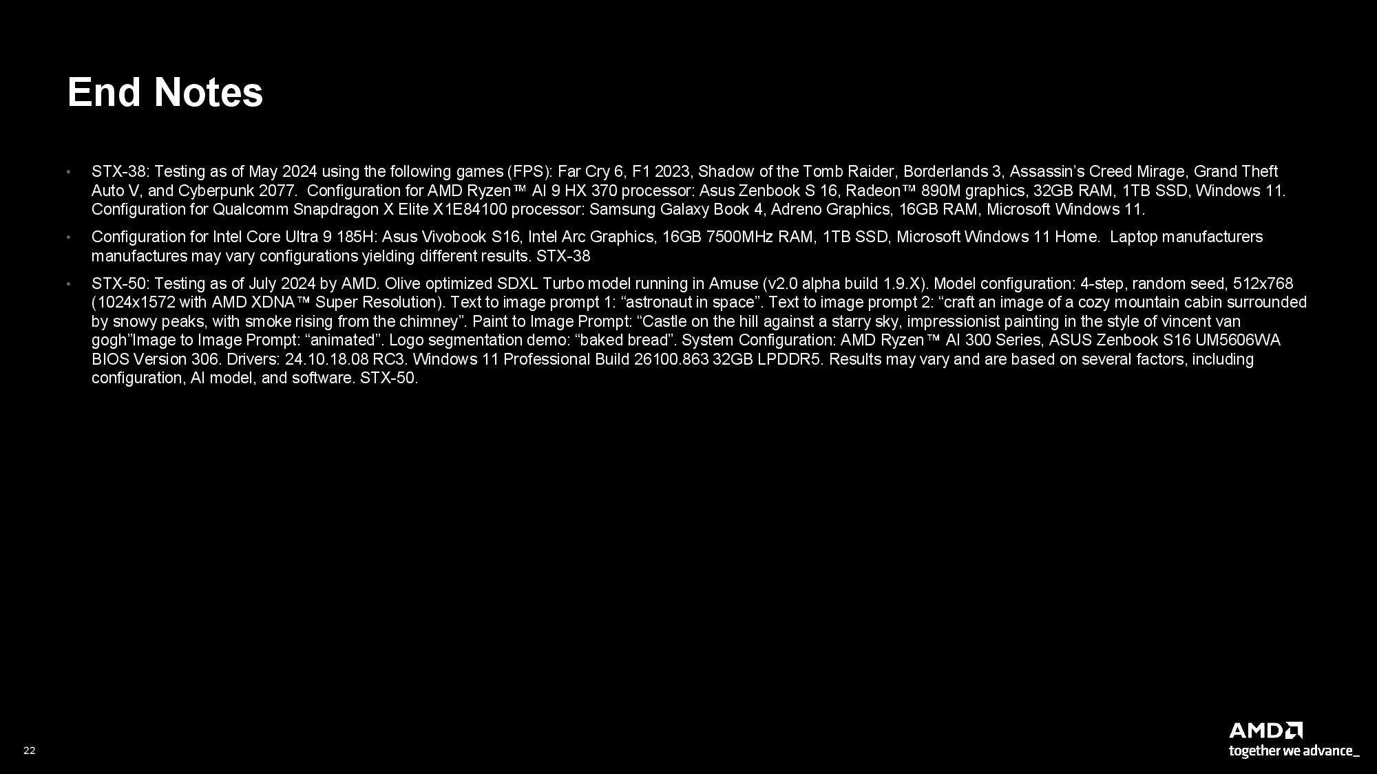
We always expect inconsistencies in vendor-provided benchmarks, so take all these results with a grain of salt. The test notes (end of the album) also indicate that the Intel processor only had 16GB of memory compared to the 32GB used for the Ryzen processor, raising the question of whether the Intel system was running in a performance-killing single-channel config — hopefully not, but the lack of a consistent configuration on the memory certainly isn't great to see.
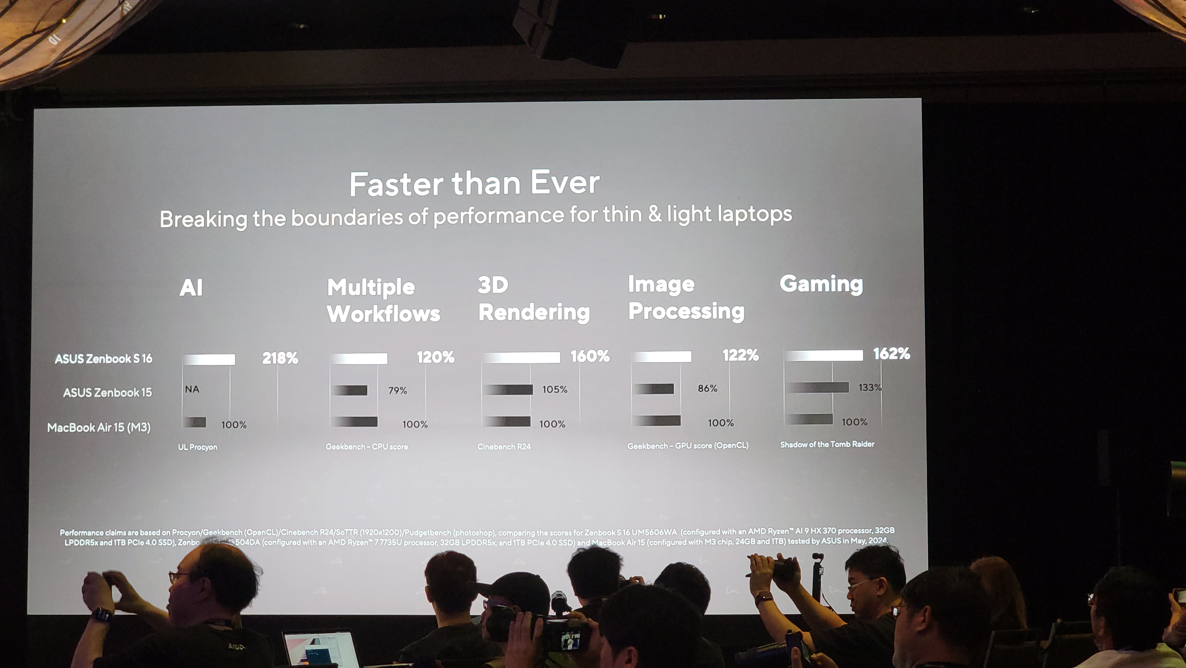
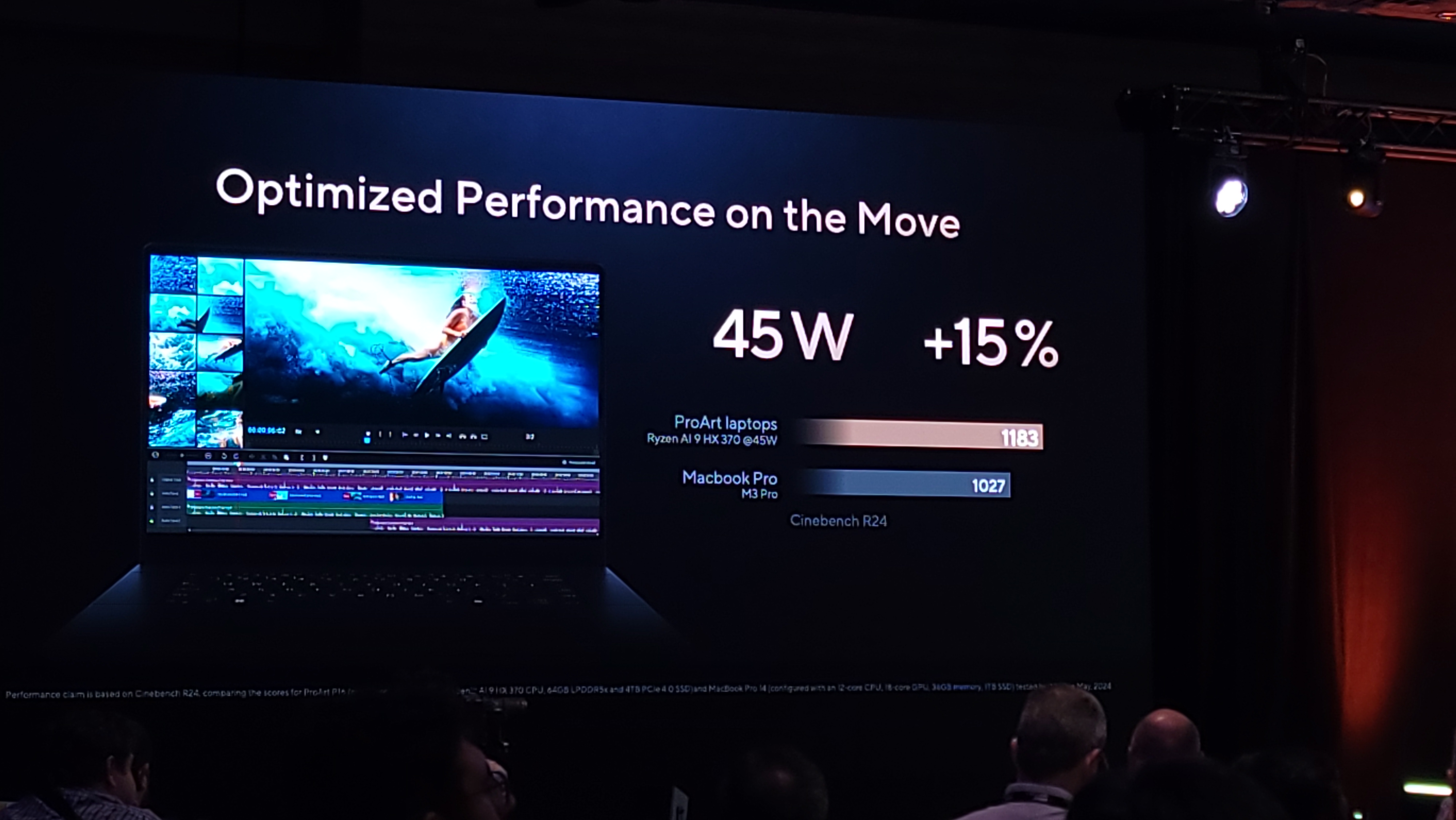
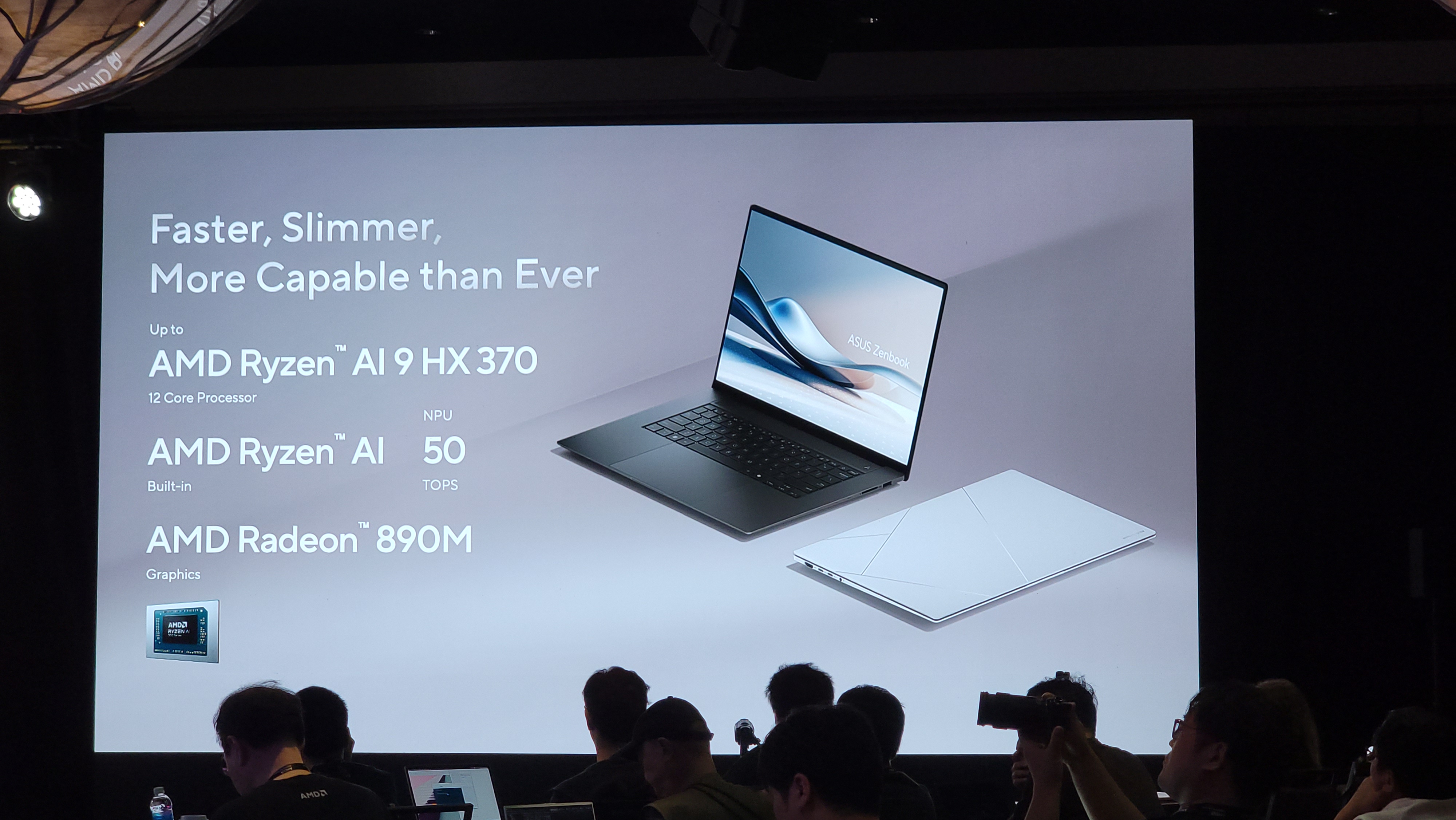
AMD has traditionally shied away from direct performance comparisons with Apple’s M series processors. However, Asus presented its new AMD-powered Zenbook S 16 at the event and shared some of its own benchmarks to highlight the Ryzen AI 9 HX 370’s performance against a competing Apple MacBook Air 15 with an M3 processor. Asus provided sparse test config info in the slide, so we’ll have to take these benchmarks with more than the usual amount of salt.
Asus claims substantial leads over the MacBook Air 15, with wins ranging from a 20% advantage in the Geekbench OpenCL CPU score benchmark to a whopping 118% lead in the UL Procyon benchmark. Other notable wins include a 60% advantage in Cinebench (certainly the multi-threaded benchmark) and a 20% lead in the Geekbench CPU score.
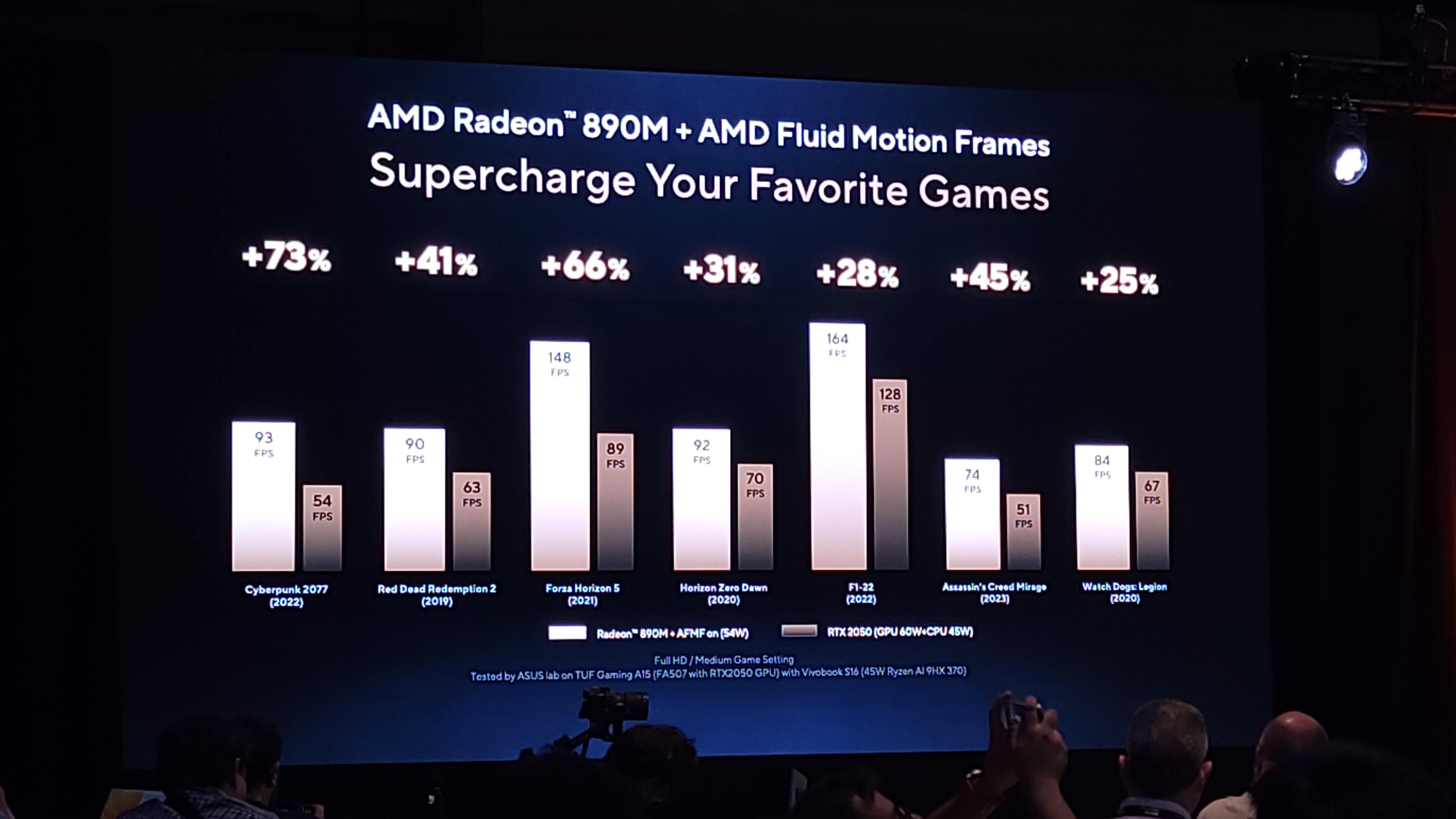
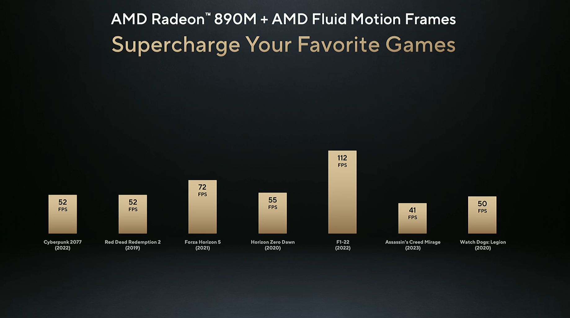
Asus also touted the performance gains to be had with AMD’s Fluid Motion Frames (AFMF) and the 54W Strix Point’s Radeon 890M integrated graphics, showing the combination delivering more performance than a discrete RTX 2050 GPU (60W GPU + 45W CPU). As you would expect, Radeon only led because of the extra frames added by AFMF, a driver-level implementation of frame generation that doesn't always work as well as charts might indicate. (We have two copies of that slide in the deck above, one with the Radeon scores without AFMF and the comparative slide with AFMF enabled.)
AMD Zen 5 Microarchitecture
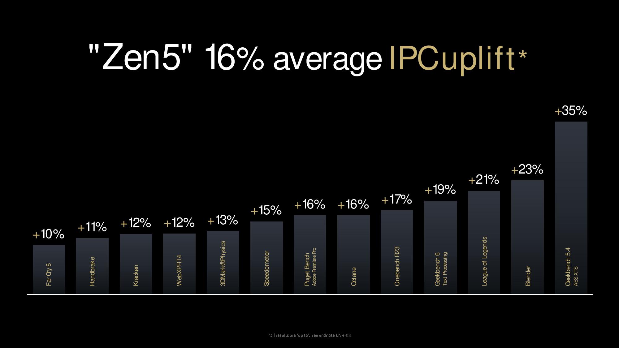
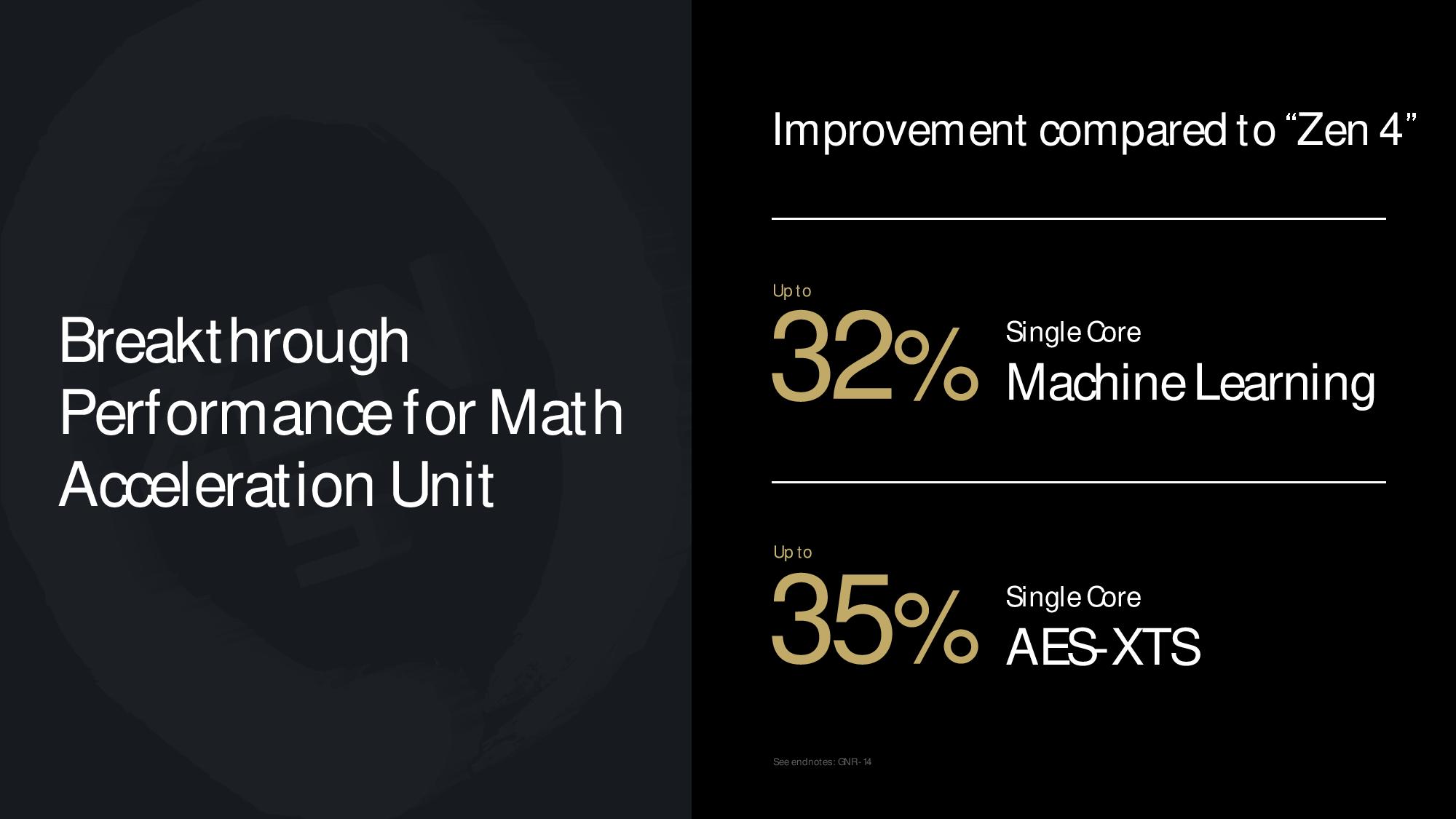
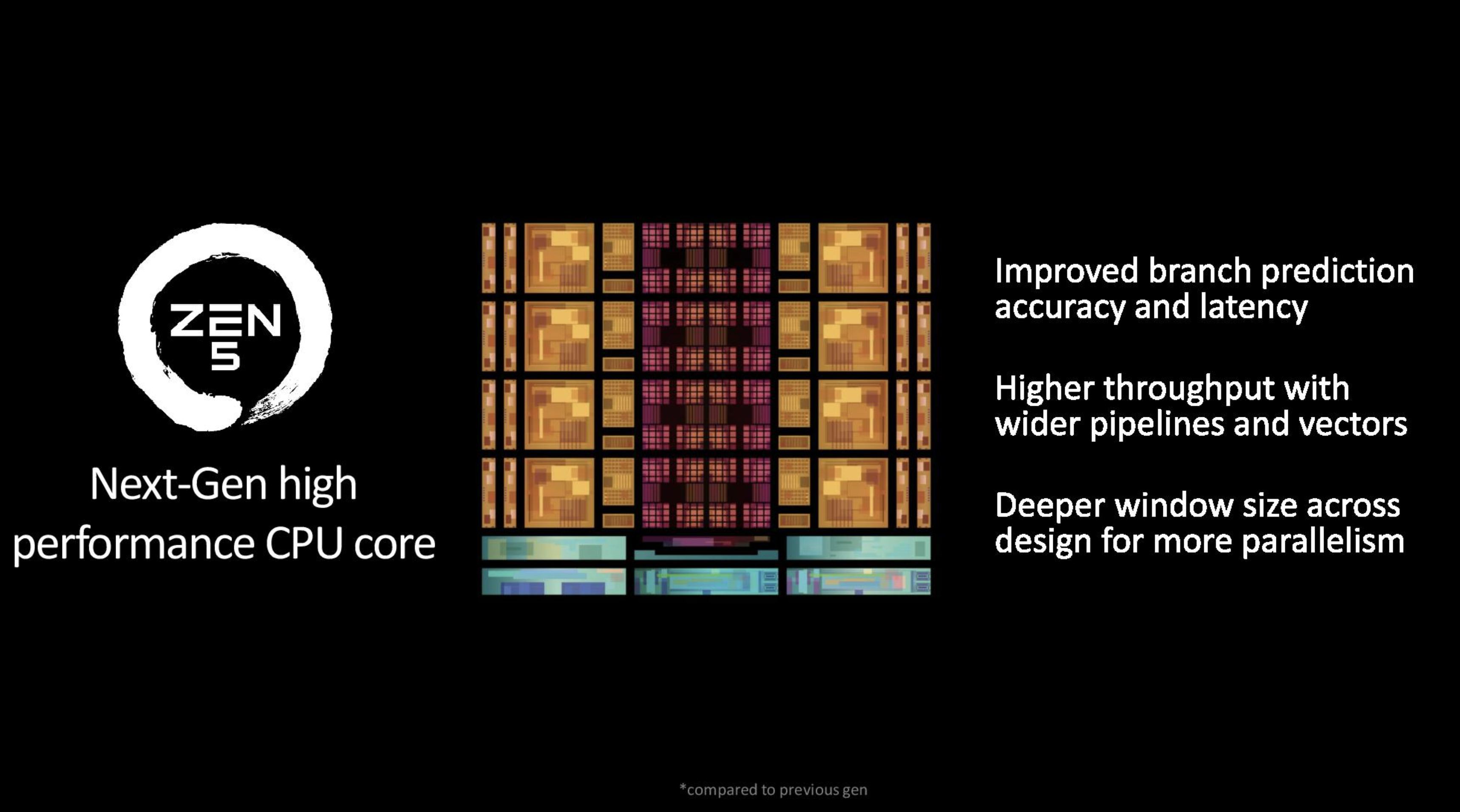
The Zen architecture debuted with a 52% IPC improvement over Bulldozer in 2017, and the company has delivered double-digit IPC increases in every generation since. Zen 5 has a 16% increase in IPC, as measured across 13 workloads. Zen 5 has dramatically improved vector math performance, with a 32% gain over Zen 4 in single-core machine learning (VNNI) and a 35% gain in single-core AES-XTS encryption workloads (AVX-512), as measured by the Geekbench subtests.
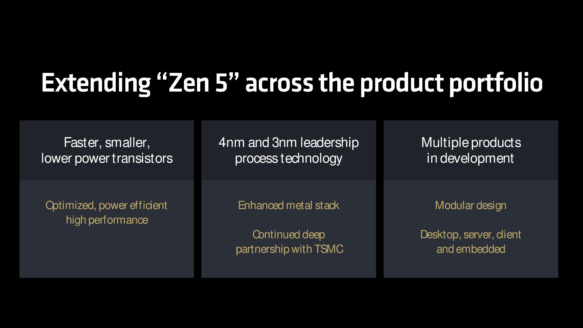
Zen 5 is an overhaul with new architectural underpinnings that its lead architect, Mike Clark, says will serve as the foundation for the next several generations of microarchitectures. It will also be used for chips with the TSMC 4nm and 3nm process nodes, with concurrent leapfrogging teams working on both designs.
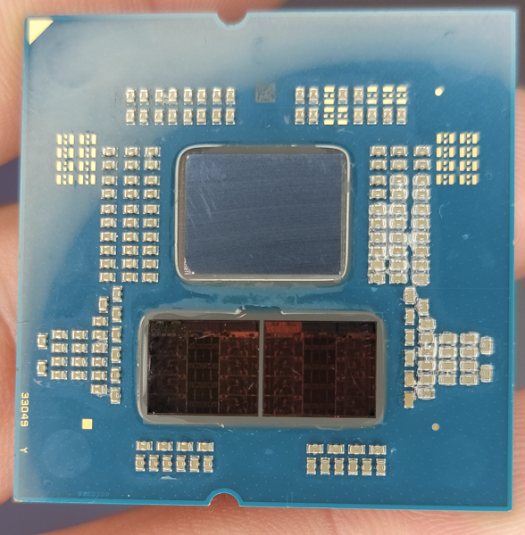
As with Zen 4 processors, the core compute die (CCD) has a maximum of eight cores and a large central 32MB shared L3 complex. Two CCDs are connected to the same 6nm I/O Die (IOD) used with the Zen 4 processors, so the chip provides the same graphics support and basic connectivity options. You can see the Ryzen 9000 diagram in the second image above.
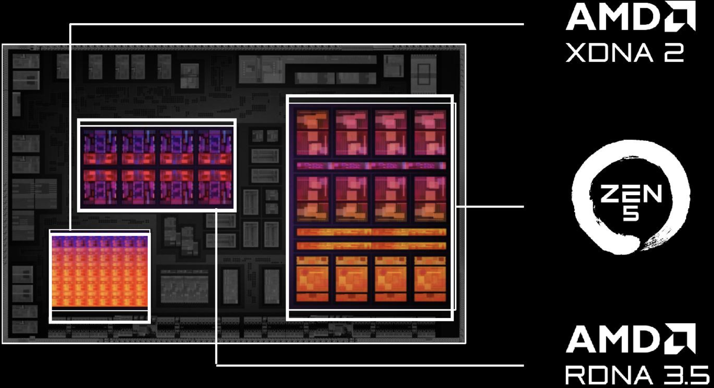
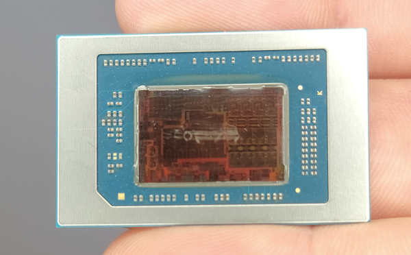
AMD didn’t share any new slides about the compact Zen 5c cores, but we teased out a few details. As a reminder, AMD's Zen 5c cores are designed to consume less space on a die than the 'standard' Zen 5 performance cores while delivering enough performance for less demanding tasks, thus saving power and delivering more compute horsepower per square millimeter than was previously possible (deep dive here).
Intel's E-Cores take a similar approach, but AMD’s Zen 5c employs the same microarchitecture as the standard Zen 5 cores and supports the same features with its smaller cores. In contrast, Intel’s design employs different architectures and feature support for each core type. The smaller Zen 5c cores operate at lower clock rates and provide less peak performance than standard cores, but they also preserve die area for other elements, like a larger GPU and NPU.
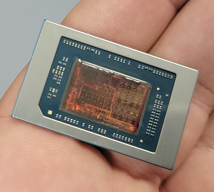
Above, you can see the previously shared image that shows the floorplan for the Ryzen AI 300 processors and the following image of the die, which has been sanded down to reveal the architecture underneath the cover. This shows the architecture in surprising detail. The four standard Zen 4 cores are aligned at the bottom of the Zen 5 cluster of cores, and the eight Zen 5C cores are aligned at the top.
Both core types have their own private L1 and L2 caches, but the 16MB of L3 cache is split into two 8MB slices, with one slice shared between the Zen 5C cores and the other slice shared between the standard Zen 5 cores (this can be seen as a single line running down the center of the eight Zen 5C cores in the block diagram).
As such, these two L3 caches have to communicate with each other over the data fabric, much like the CCX-to-CCX cache coherency mechanism found with AMD’s older Zen 2 architecture. This does introduce higher latency for cache-to-cache transfers, which AMD says is “not any more than you would have to go to memory for.” As such, AMD uses Windows scheduler mechanisms to attempt to constrain workloads to either the Zen 5 or 5C cores to reduce the occurrence of high latency transfers, with background workloads typically being assigned to the 5C cores. AMD will study behavior in the real world with concurrent apps running on both types of cores, thus continually assessing whether it would make sense to unify the L3 cache in future designs.
The design ties the three compute engines — CPU, NPU, and GPU — together with a data fabric. Each of the CPU clusters (Zen 5 and 5C) has a 32B/cycle interface, while the GPU has four 32B/cycle interfaces into the data fabric, and the XDNA engine has a single 32B/cycle interface.
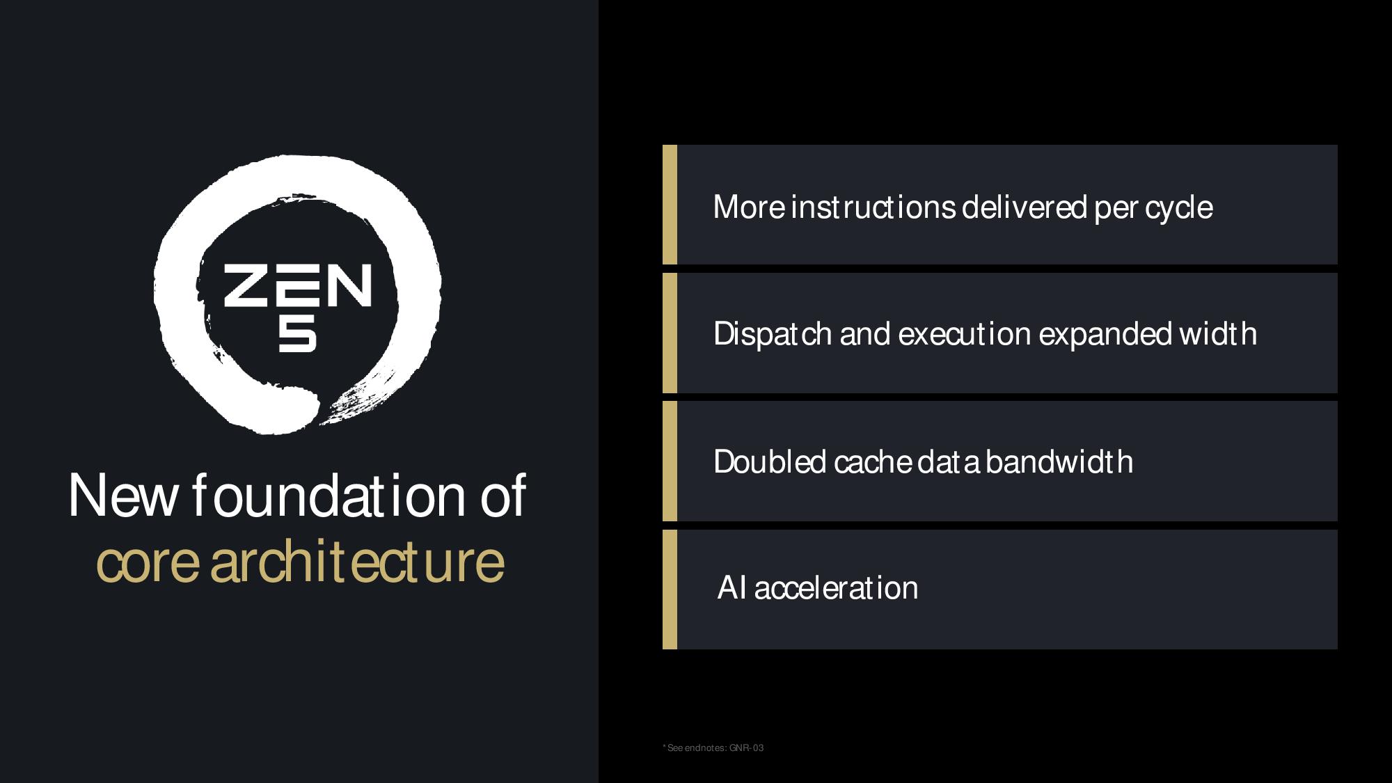
AMD redesigned the front end of the design with improved fetch, decode, and dispatch elements to feed a wider execution engine. It also doubled the data bandwidth between its L2 and L1 caches and the L1 to floating point unit, which it says helps deliver the generational gaming performance improvements.
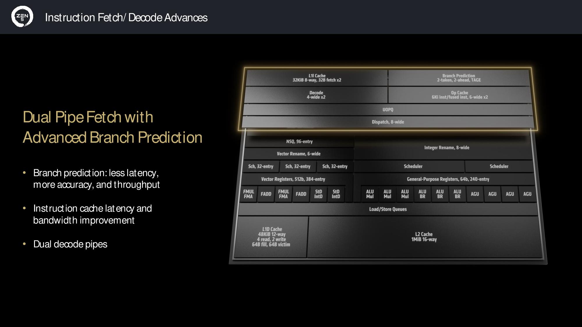
The front end features a dual pipe fetch and improved branch prediction accuracy that fuels feeding more predictions per cycle (TAGE branch prediction engine). Those predictions are fed into what are now dual-ported instruction and operation caches, which reduces latency. AMD also added a dual 4-wide decode path that feeds the micro-op queue, then the eight-wide dispatch.
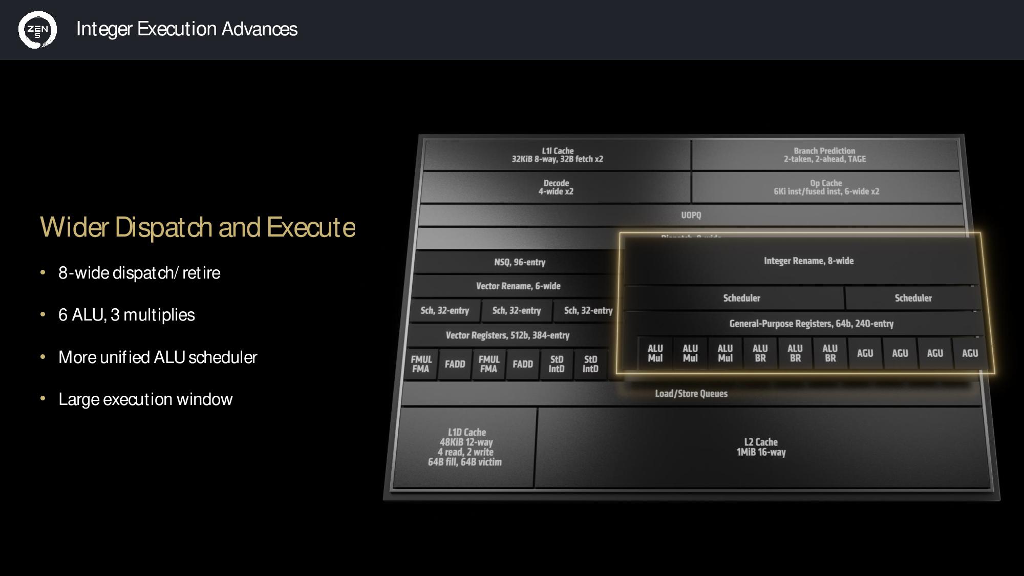
The Zen execution engine has long supported up to six instructions per cycle and four Arithmetic Logic Units (ALUs) for integer execution. Zen 5 marks the first time AMD has widened the Zen execution engine to support dispatching and retiring up to eight instructions per cycle, thus satisfying the increased instruction throughput from the front end.
Zen 4 had four schedulers for the integer unit, but Zen 5 has a unified ALU scheduler for all six ALU units. The execution window has also been widened by 40% (up to 448 outstanding ops) to better handle the extra misses that are a natural byproduct of the wider dispatch and execution.
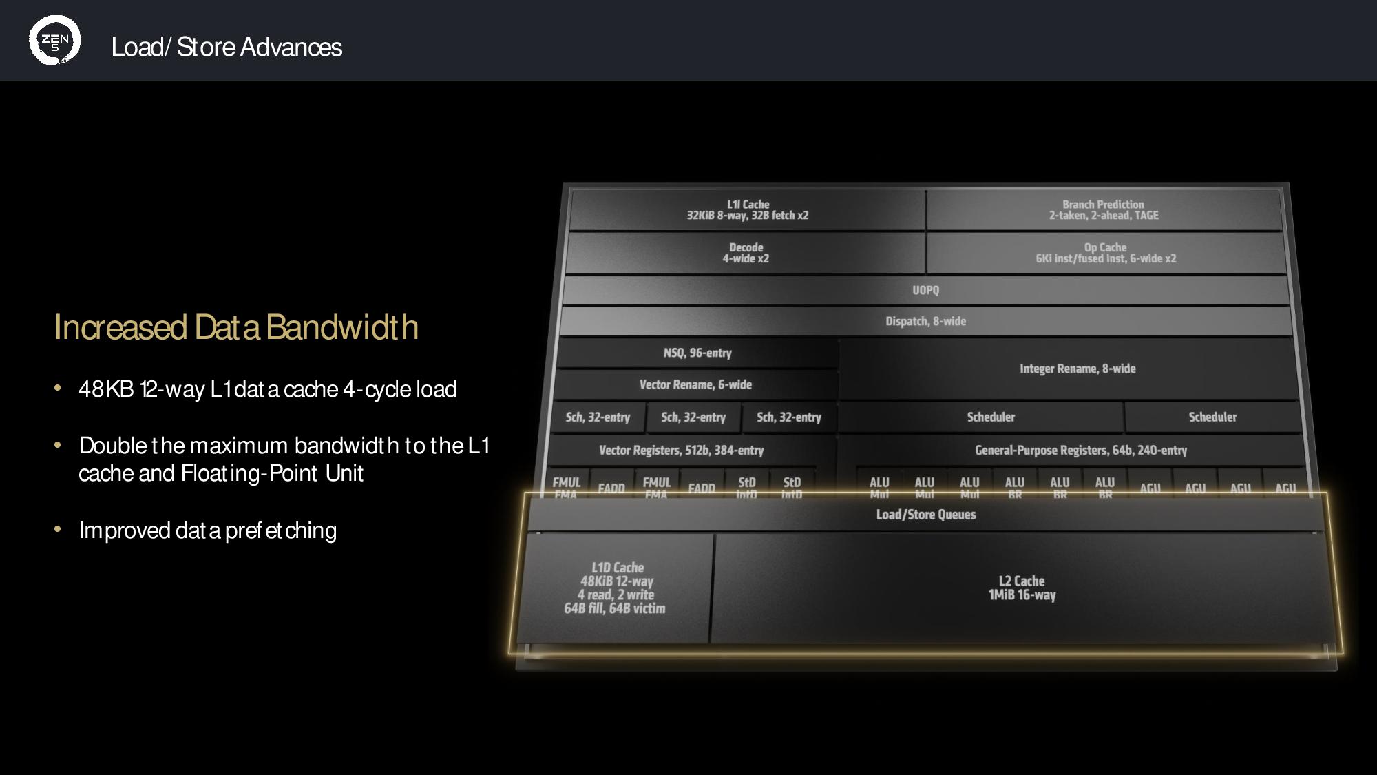
Zen 4 had a 32KB data cache, which has now been expanded to a 48KB 12-way L1 data cache (L1D) for Zen 5. Despite the increased capacity of the L1D, the unit maintains its 4-cycle load latency. Doubled bandwidth to the L1 cache and floating point unit is a crucial accommodation for the expanded AVX engine, which now supports a full 512-bit path.
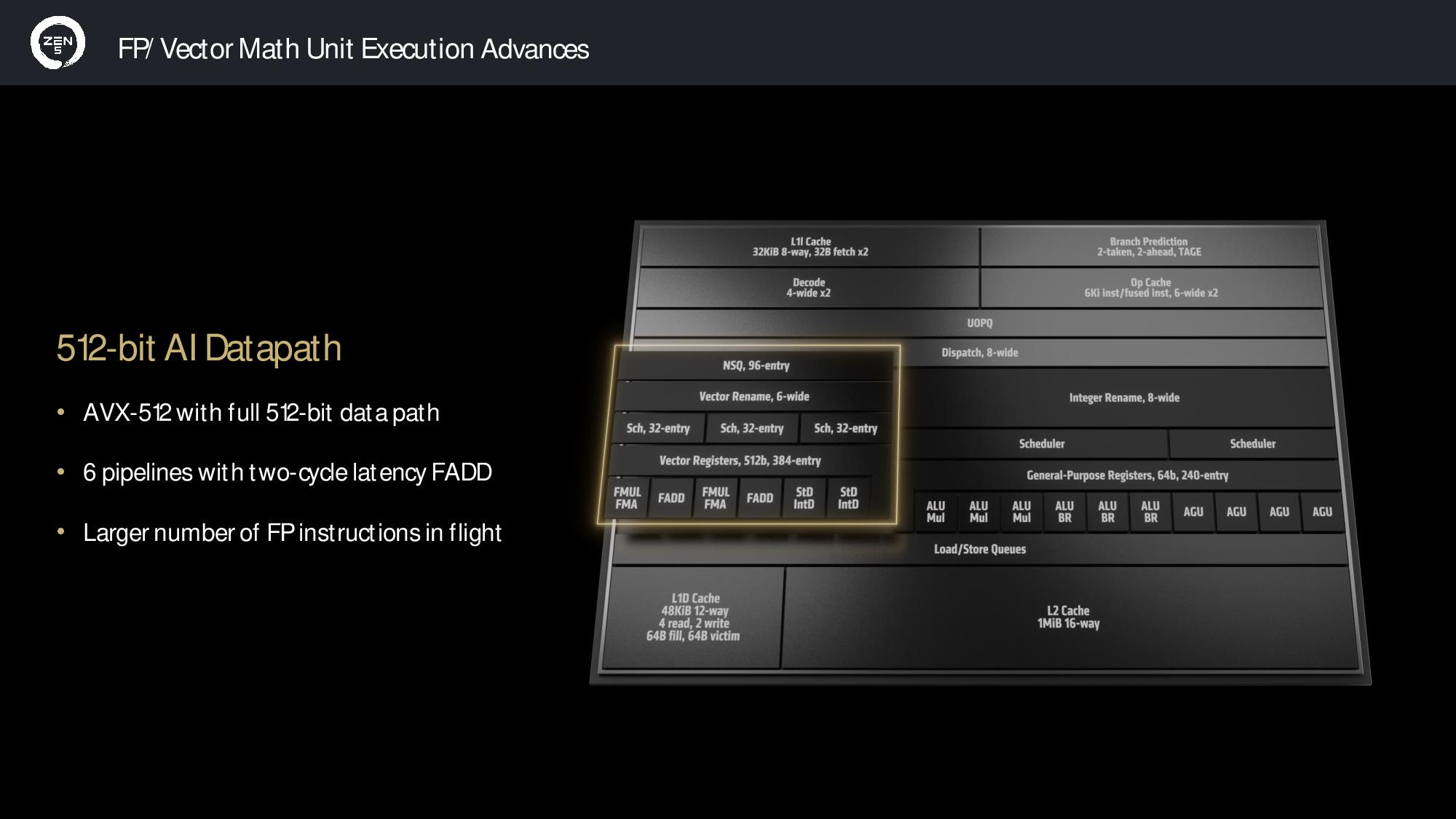
Zen 4 used a dual-issue AVX-512 pipeline (“double-pumped” in AMD parlance), wherein it essentially issued an AVX-256 instruction twice across a 256-bit interface to provide most of the performance benefits of AVX-512 while avoiding the impact to die area and resulting frequency drops.
Zen 5 supports the full 512-bit data path to deliver doubled AVX-512 and VNNI throughput, but AMD says the chip still runs at its full frequency for any given multi-core workload during AVX-512 work. That stands in stark contrast to Intel’s AVX implementation, which results in severe frequency reductions.
AMD’s vector math unit is also modular, and it still supports the ‘double-pumped’ 256-bit option for its APU designs. AMD also reduced the latency for a floating point add (FADD) from three cycles to two, improving performance.
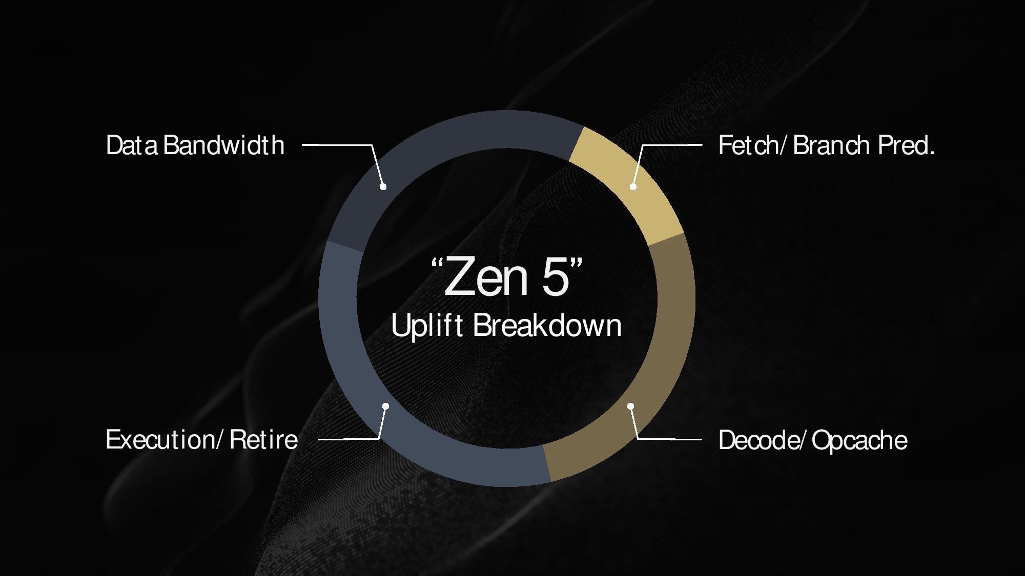
AMD quantified several of the various contributors to its 16% IPC improvement, with 34% of the gain being contributed by the move to an 8-wide execution/retire pipelines, 27% each from the decode/opcache and data bandwidth improvements, with the remaining 12% coming from the enhanced fetch/branch prediction.
AMD RDNA 3.5
AMD’s RDNA 3.5 engine powers the Radeon 890M and 880M integrated graphics in the Strix Point processors, but AMD doesn’t use it for the Ryzen 9000 processors — those continue to leverage the RDNA 2 architecture.
AMD’s Mark Papermaster credits the company’s partnership with Samsung, wherein the company licensed its RDNA graphics IP for use in Galaxy smartphones, as a key source of learning about low-power environments. Those same lessons are very useful for other mobile designs, like laptops, that are also limited by battery power.
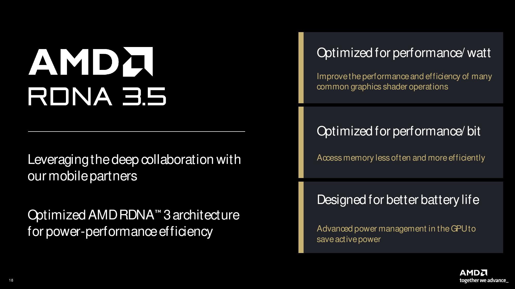
AMD incorporated those lessons into RDNA 3.5, an incremental change to the RDNA 3 engine that infuses a series of optimizations that improve performance per watt through several techniques, including targeted changes to the texture and shader engines. The design also improves performance per bit with an optimized memory subsystem. Papermaster says these alterations yielded a "double-digit performance gain" per unit of energy expended.
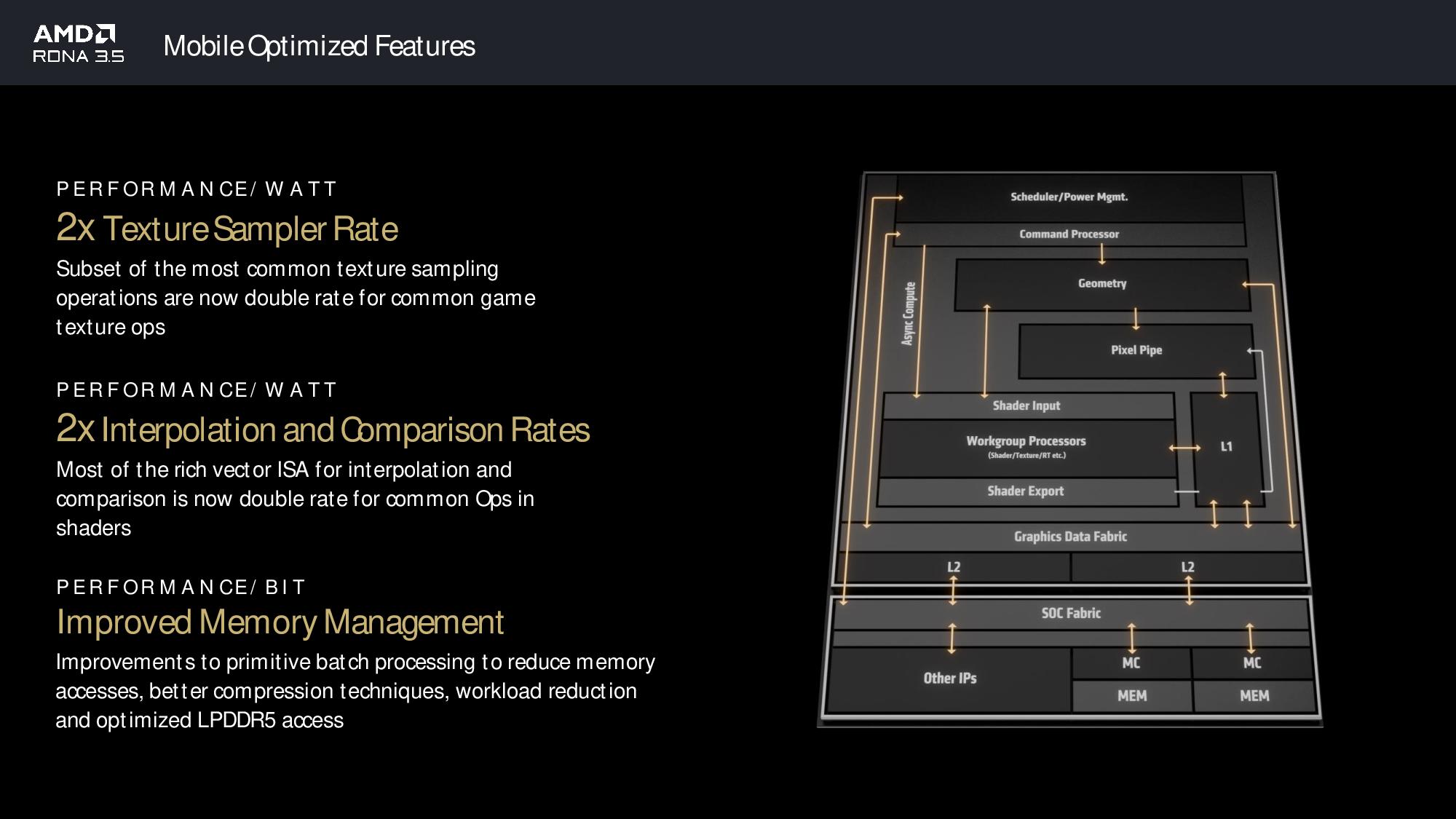
Other improvements include a doubled texture sampler rate that was accomplished by doubling the number of texture sample units to introduce more parallelism for game texturing. AMD also doubled the pixel interpolation and comparison rates and added a scalar arithmetic logic unit to identify single-use write operations, which it then discards to boost performance and efficiency. Papermaster also pointed to an entirely new method of creating smaller sub-batches that reduces access to LPDDDR5 memory and optimized memory compression to reduce data traffic, both of which save power while improving performance.
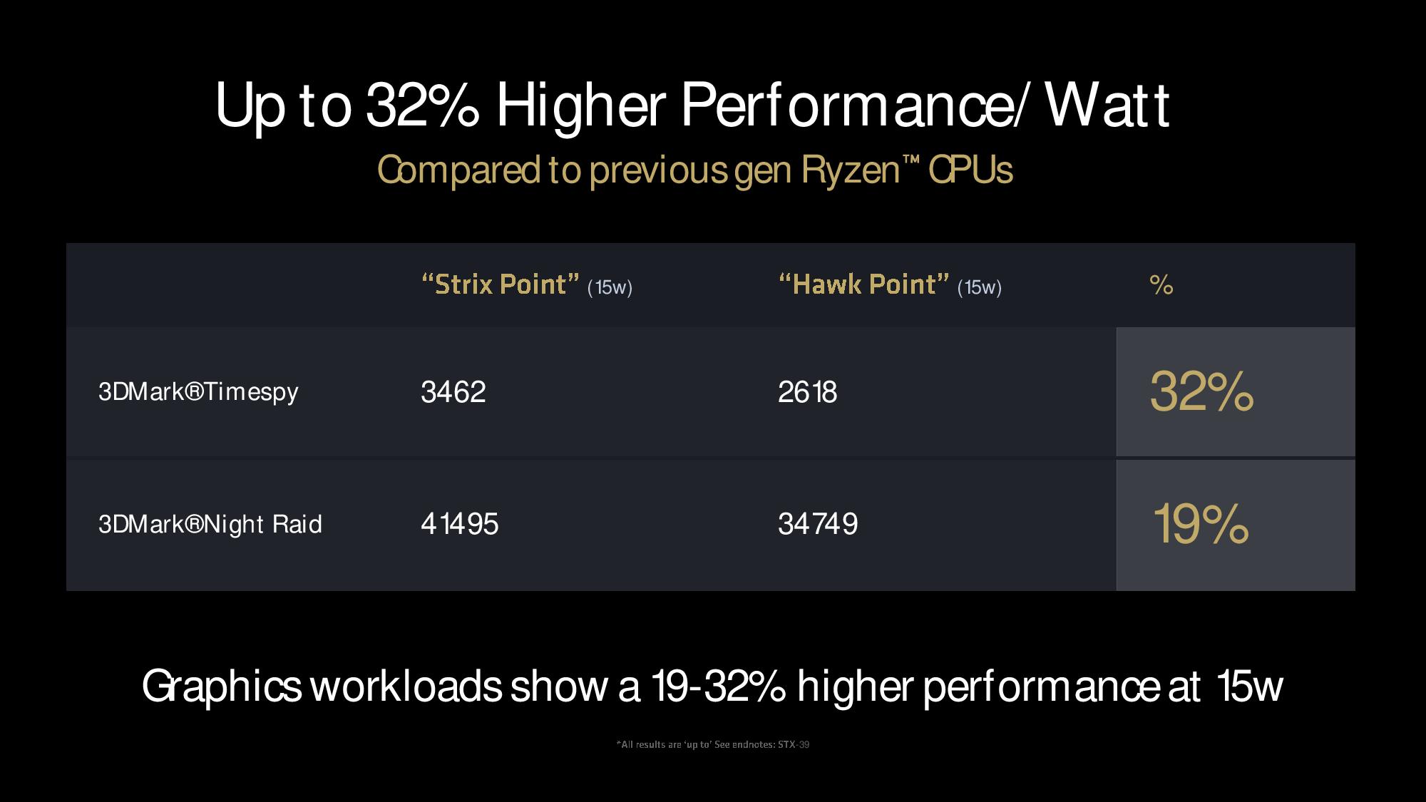
AMD claims the combined optimizations yield a 32% improvement in power efficiency for a Strix Point processor running at 15W in the 3Dmark Timespy benchmark over a Hawk Point chip also running at 15W. AMD’s tests also showed a 19% improvement in power efficiency in the 3Dmark Night Raid benchmark. Remember however that these are purely synthetic workloads that aren’t the best proxy for real-world gaming performance or efficiency.
AMD XDNA 2 NPU Architecture
AMD’s Ryzen AI 300 series is the company’s third generation of processors with an in-built neural processing unit (NPU). AMD’s Phoenix chips were the first x86 processors with an in-built NPU, delivering 10 TOPS of performance via the XDNA NPU, and AMD improved that to 16 TOPS with the second-gen Hawk Point models. However, those gains came from increased clock speeds instead of changes to the XDNA architecture.
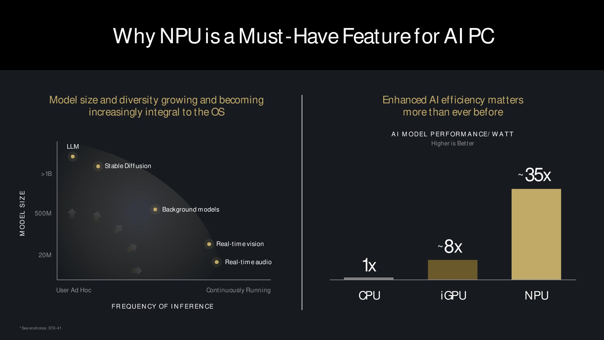
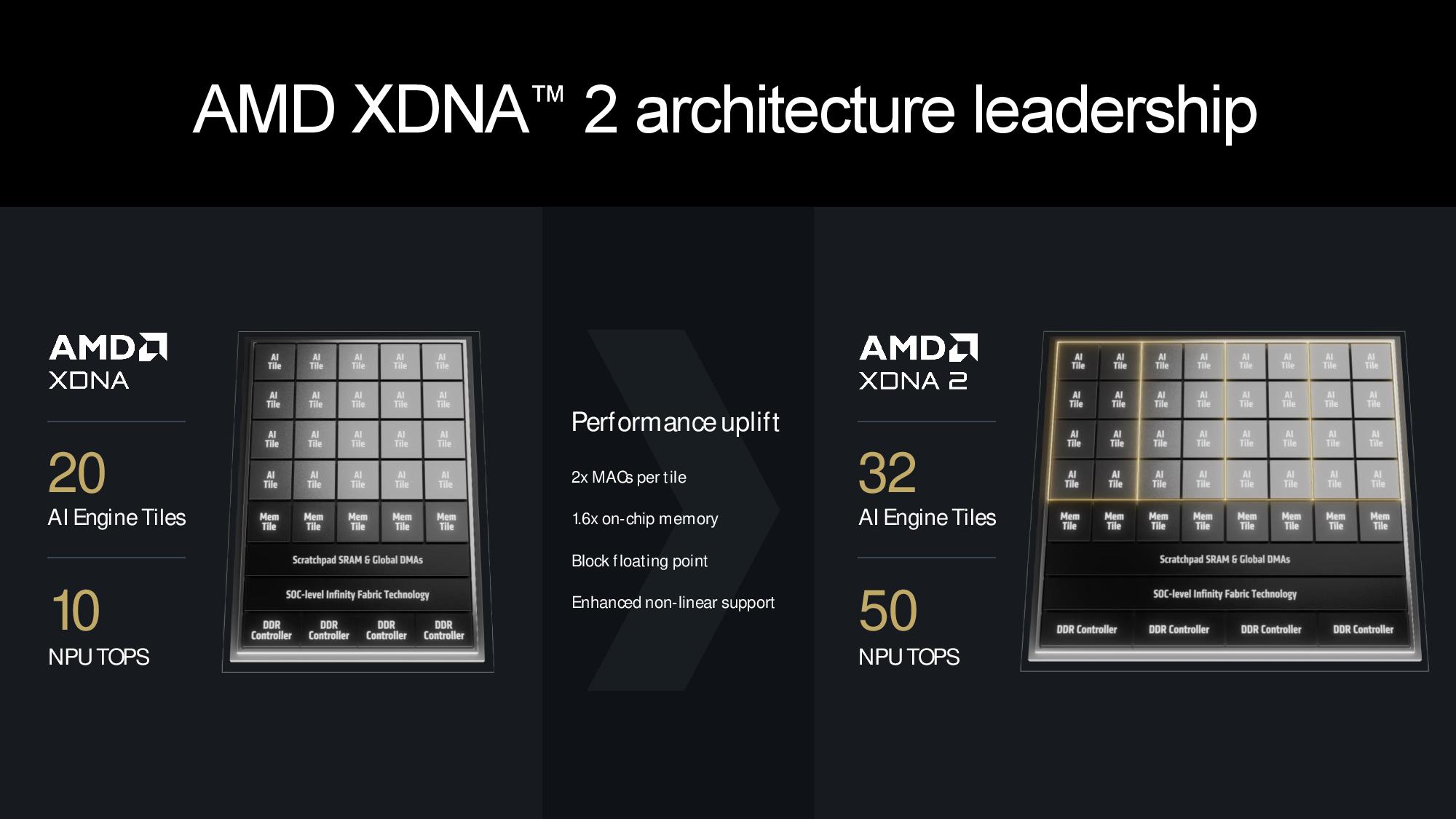
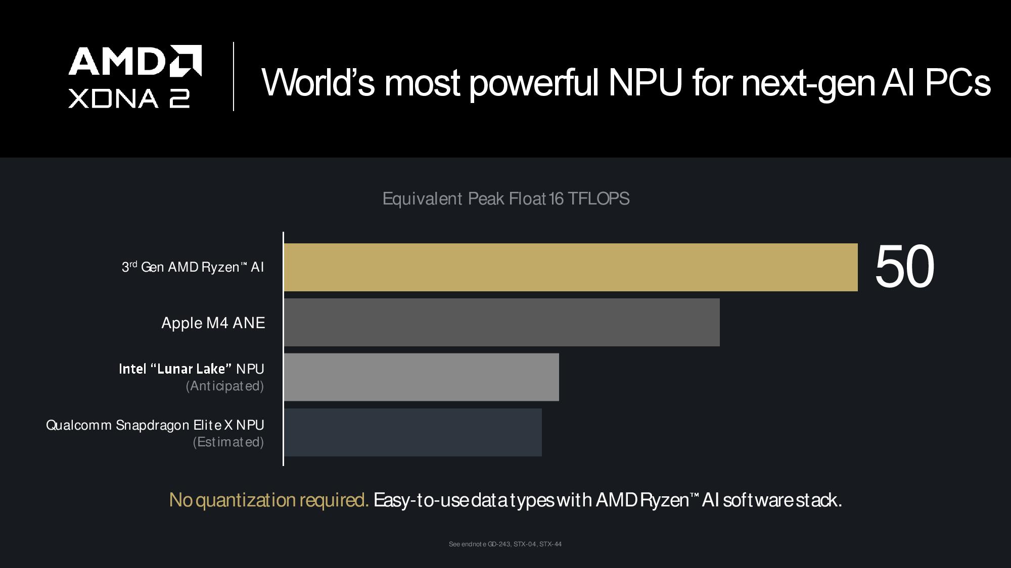
Strix Point moves forward to 50 TOPS of NPU performance with the second-gen XDNA 2 engine, a tech borne of AMD’s Xilinx acquisition. Going beyond the speeds and feeds, above, we can see one of the biggest rationales for native AI acceleration — power savings. Here, AMD shows that its XDNA 2 engine is up to 35X more power efficient at running an AI model than the CPU, and that capability becomes more critical for long-duration background workloads, the sweet spot for NPUs.
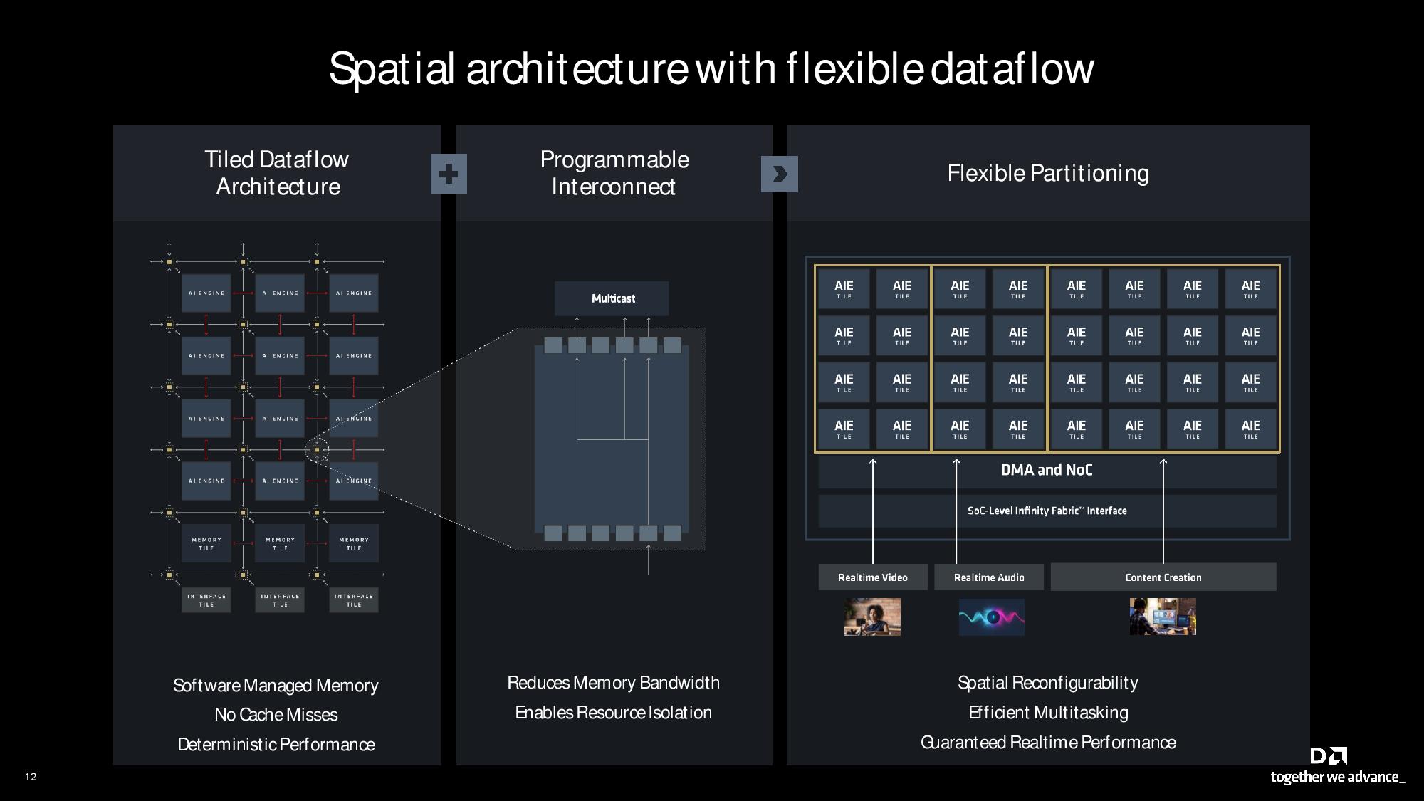
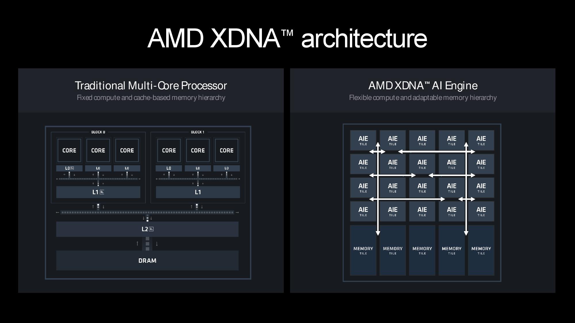
The XDNA 2 engine is a spatial dataflow architecture with a 2D array of compute tiles tied together with a flexible interconnect that can be programmed at run time to create custom compute hierarchies. AMD says all other NPUs have a fixed hierarchy and don’t have the terabytes of east/west bandwidth available in XDNA 2's interconnect fabric. The architecture also employs SRAM buffers placed throughout the array. AMD claims the cache-less design offers very deterministic latency — key for AI workloads — and the programmable interconnect maximizes bandwidth by allowing seamless data multicasting between units to reduce traffic on the fabric.
The design also supports flexible real-time portioning. For instance, a single column of AIE compute tiles can be dedicated to a light workload, while a quad-column array can be assigned to a heavier task. This technique is designed to optimize power, performance, bandwidth, and latency while running concurrent AI models.
Architectural enhancements have added plenty of processing horsepower per tile, but AMD also had to expand the number of tiles from 20 to 32 to reach the full 50 TOPS target. The company also added 1.6X more on-chip memory and twice the number of MACs (multiply accumulators) per tile.
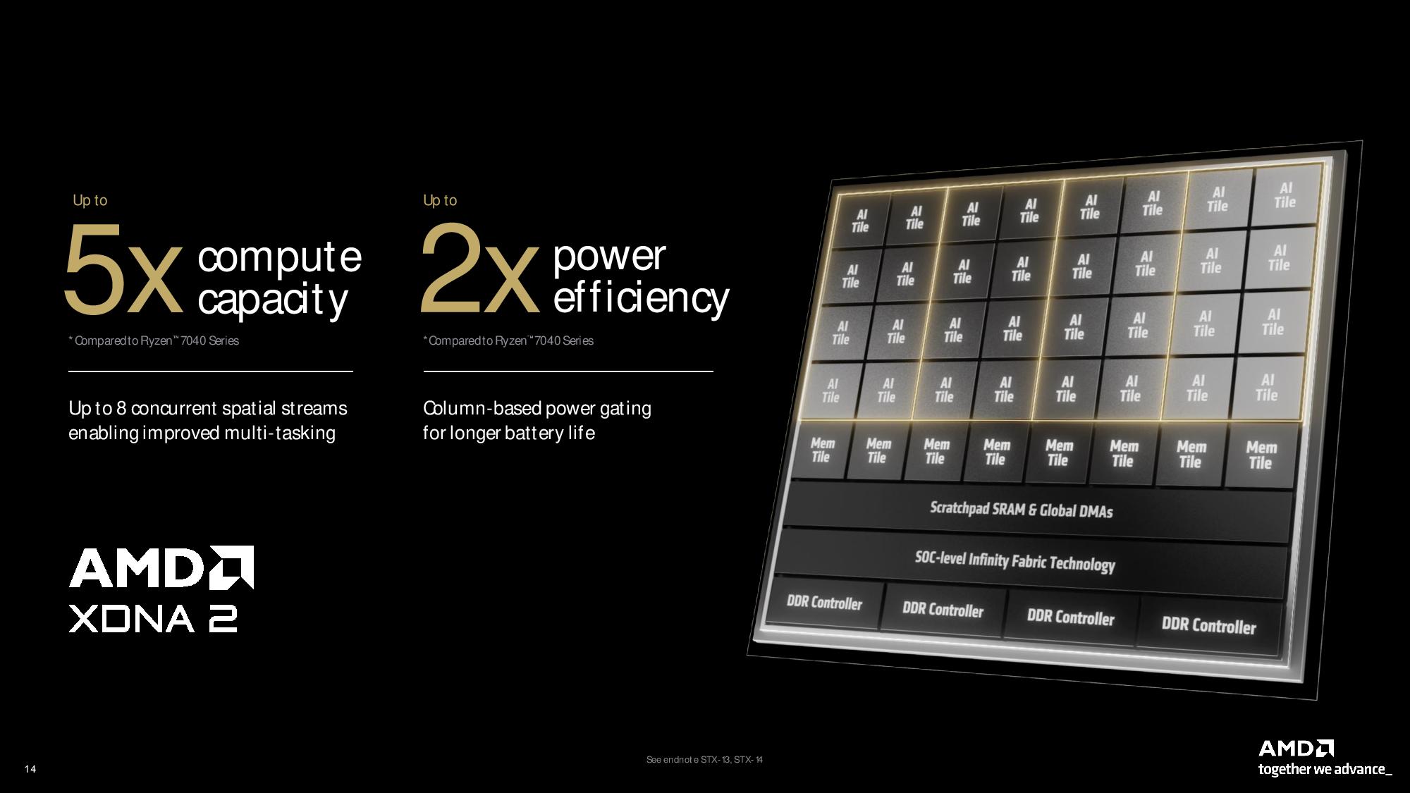
The architectural changes with the XDNA 2 engine result in up to five times the compute capacity and twice the power efficiency of the first-gen XDNA engine. XDNA 2 also supports running up to eight concurrent AI models.
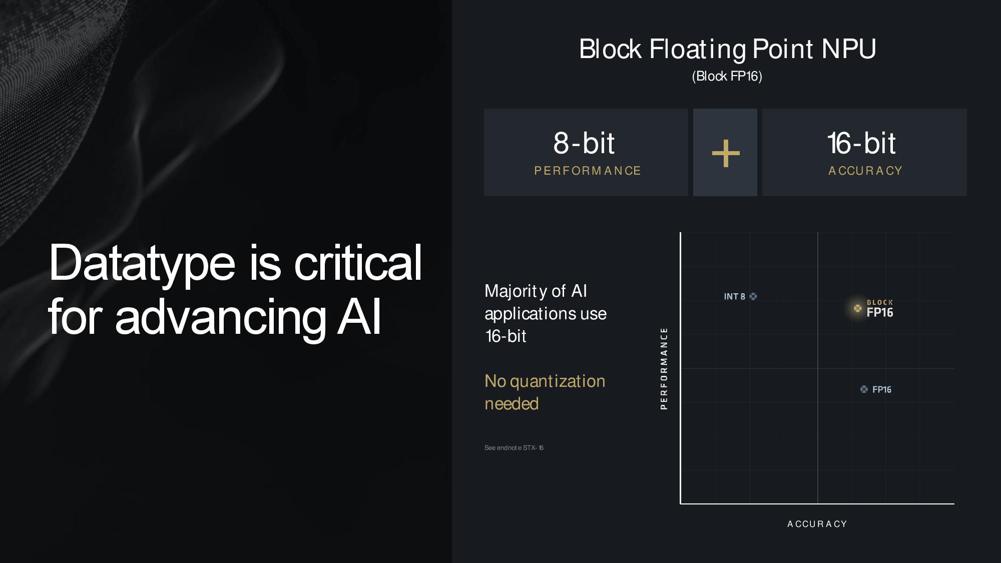
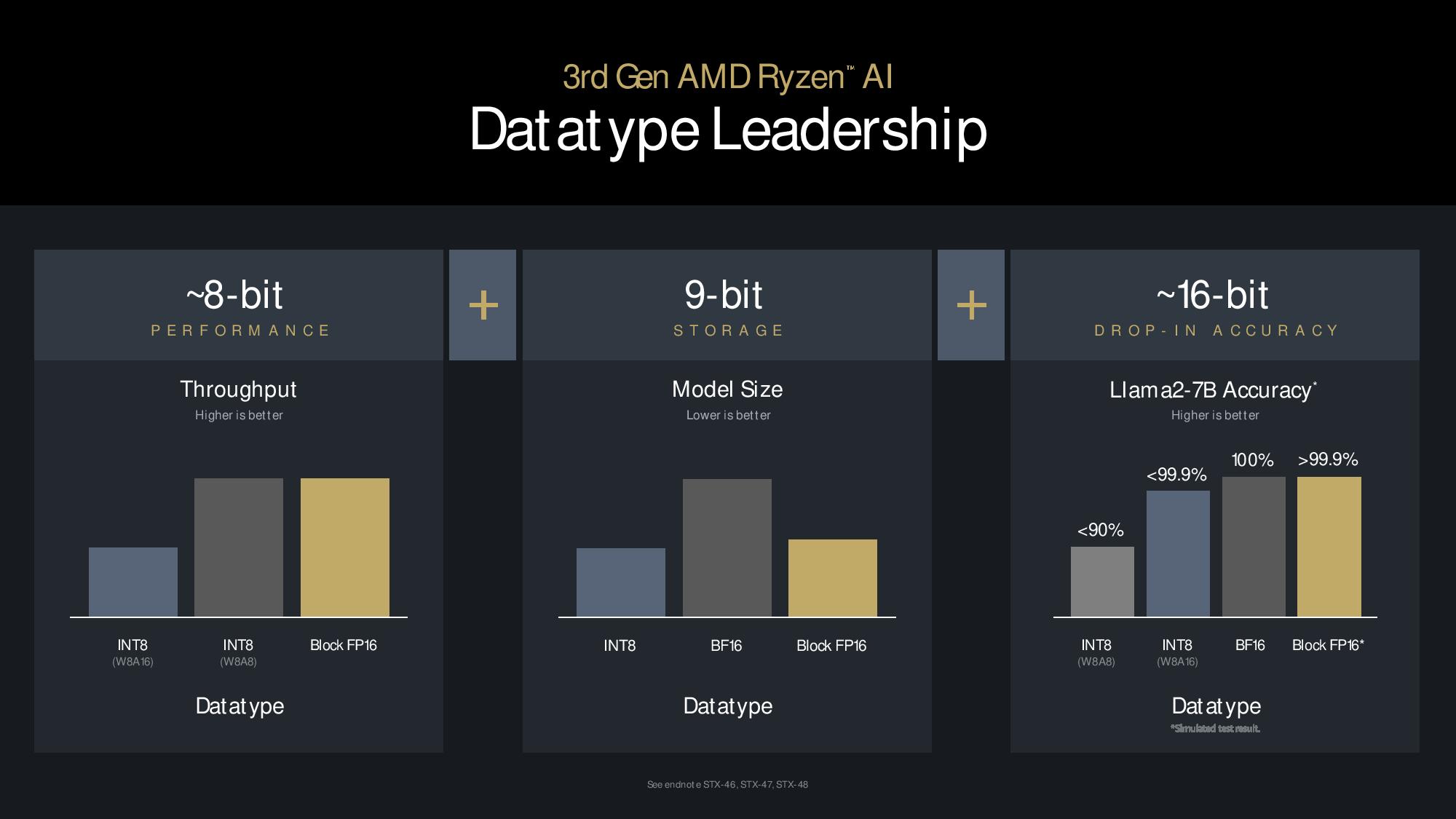
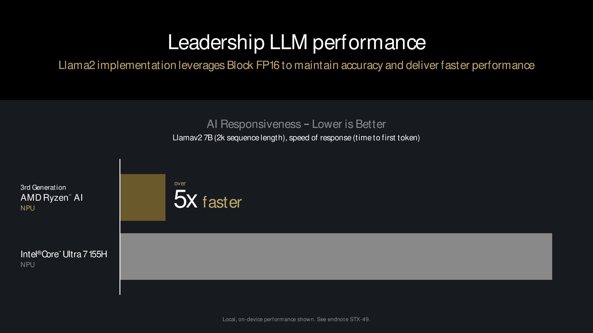
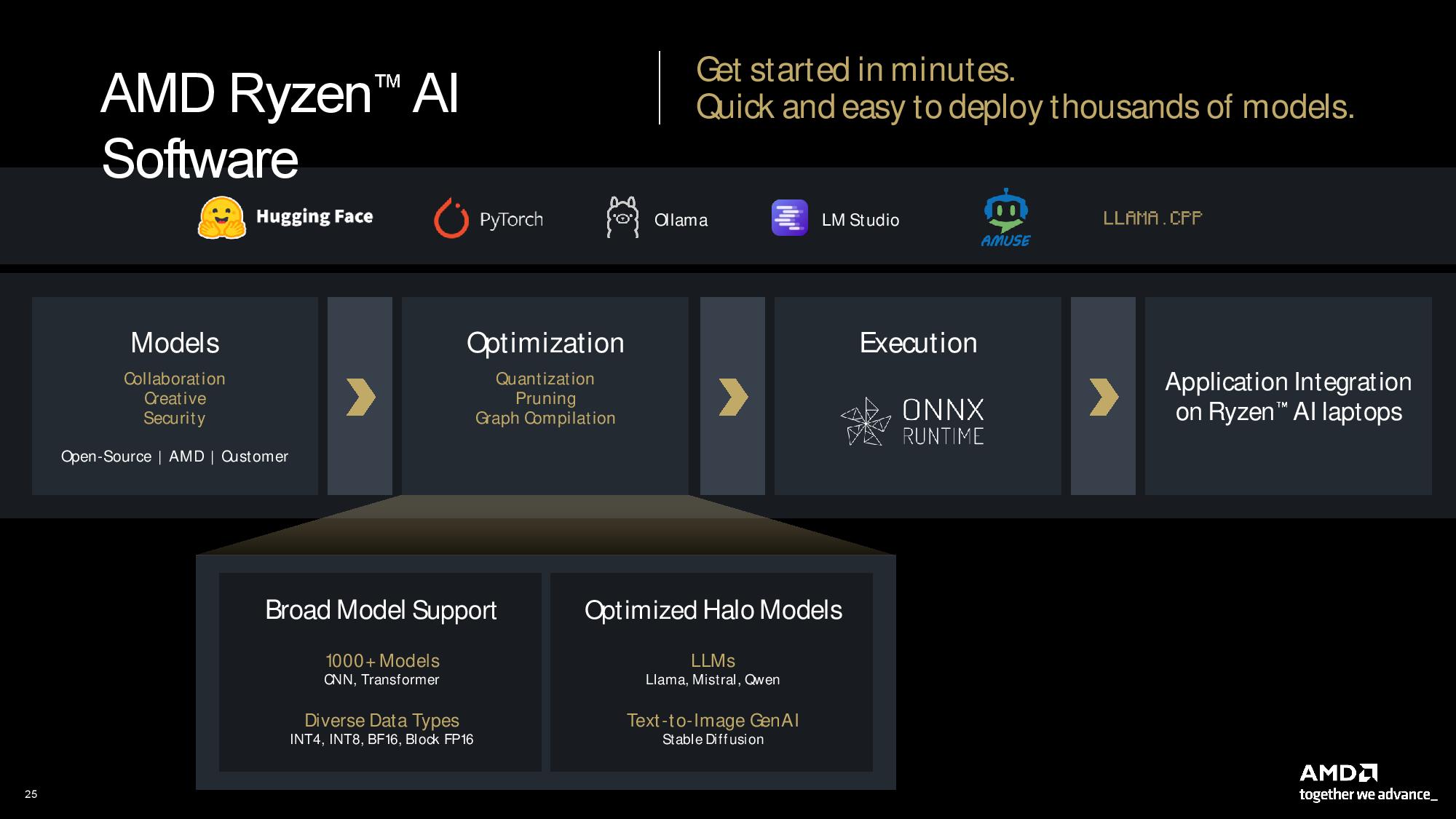
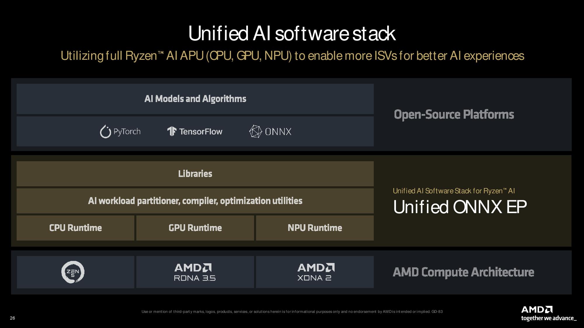
NPU performance is typically measured by performance in INT8 workloads, a less precise data type that uses less computing and memory to run a model. However, models must be quantized to the INT8 format first, and they lose some precision in the process.
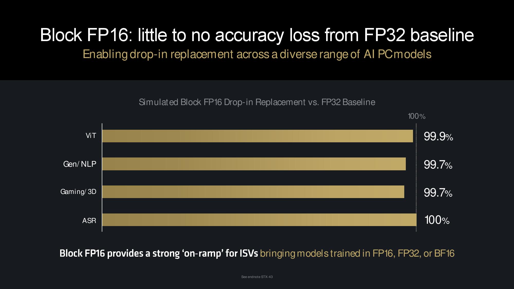
AMD’s XDNA 2 NPU supports Block BF16, a new data format that is said to provide the full accuracy of FP16 with many of the same compute and memory characteristics as INT8. AMD says Block FP16 is plug-and-play with its implementation; it doesn’t require quantizing, tuning, or retraining of existing models.
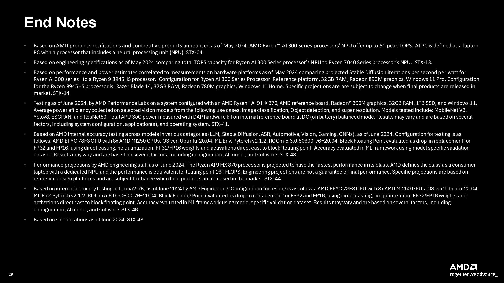
AMD claims to have the only NPU on the market supporting Block FP16, but Intel has said Lunar Lake also supports the math format. AMD’s representatives didn’t seem familiar with Intel’s support for the format, and they acknowledged that this would invalidate their Lunar Lake performance projections in the benchmarks above.
Thoughts
The Ryzen 9000 'Granite Ridge' processors arrive on July 31, an opportune time. Intel is struggling with widespread crashes with its flagship enthusiast processors, an unresolved problem, and its competing Arrow Lake processors won't come to market until later in the year. That could potentially leave AMD with the performance crown for several months. Ryzen 9000 is coiled to take on Intel’s coming chips, with the 16% IPC increase floating all boats in terms of performance, while the up to 40% reduction in TDP for the lower-tier models capitalizes on AMD’s power consumption advantages.
However, Arrow Lake will be a stiff competitor — it will be the first to come with Intel’s new 20A process node. This node features Intel's first backside power delivery (PowerVia) and gate-all-around (GAA/RibbonFET) transistors. The chips are also said to come with the new Lion Cove P-cores and Skymont E-cores, again marking another significant step forward that should keep competition heated in the desktop PC market.
Laptops with AMD’s Ryzen AI 300 ‘Strix Point’ processors will be available on shelves this month, and that couldn’t come at a better time — Qualcomm’s Snapdragon X Elite Arm processors have stolen the show with the distinction of being the only systems that meet Microsoft’s requirements to be branded as a Windows Copilot+ PCs.
It appears that AMD’s official Copilot+ certification won’t come until later in the year. Still, the ability to field AI-capable PCs with higher TOPS performance from the NPU, even if only five additional TOPS, is a marketing win that will help keep AMD in the limelight of the AI PC upgrade craze. AMD also has the distinction of beating Intel’s Lunar Lake to market, leaving it some breathing room for now. And AMD doesn't need to worry about x86 emulation or graphics driver woes, something that Qualcomm continues to work on.
The Zen 5 Ryzen 9000 'Granite Ridge' processors arrive on July 31, and Ryzen AI 300 'Strix Point' laptops will also be on shelves by the end of the month. Stay tuned for the real tale of the tape when we post our reviews later this month.


