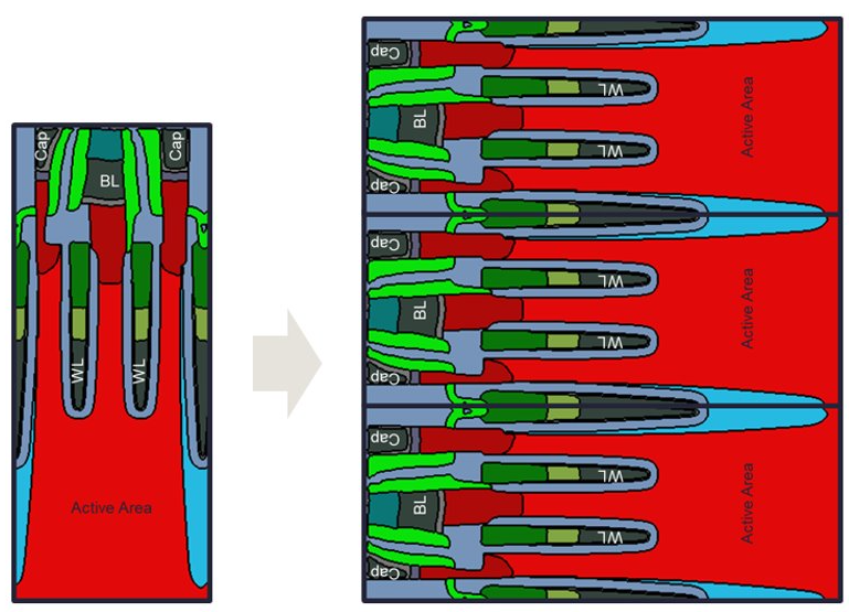
If there's one tech product where scaling doesn't work quite as well, it's DRAM. There are a number of reasons for this, the most important being the actual design of DRAM cells and how it relates to fabrication. But according to Lam Research, the end result of these scaling difficulties means that researchers in the DRAM field may be out of ways to increase DRAM's density scaling as early as five years from now.
It's in this context that Lam Research, a company specializing in semiconductor circuit design, has published a proposal for how future DRAM products may evolve. And that future may very well be 3D, so it seems that memory cubes aren't that far outside the realm of possibilities. According to the company, it'll take us around five to eight years to be able to design a manufacturable 3D DRAM device, leaving the world with a possible three-year gap between the moment 2D DRAM scaling ends and 3D DRAM scaling picks up.
Using their proprietary SEMulator3D software, Lam Research iterated on possible 3D DRAM designs. Their focus was on solving scaling and layer stacking challenges, capacitor and transistor shrinking, inter-cell connectivity, and via arrays (such as TSMC's TSV [Through Silicon Vias], which we've seen in other 3D semiconductor designs already). Finally, the company laid down the process requirements that enable fabrication of their proposed design.