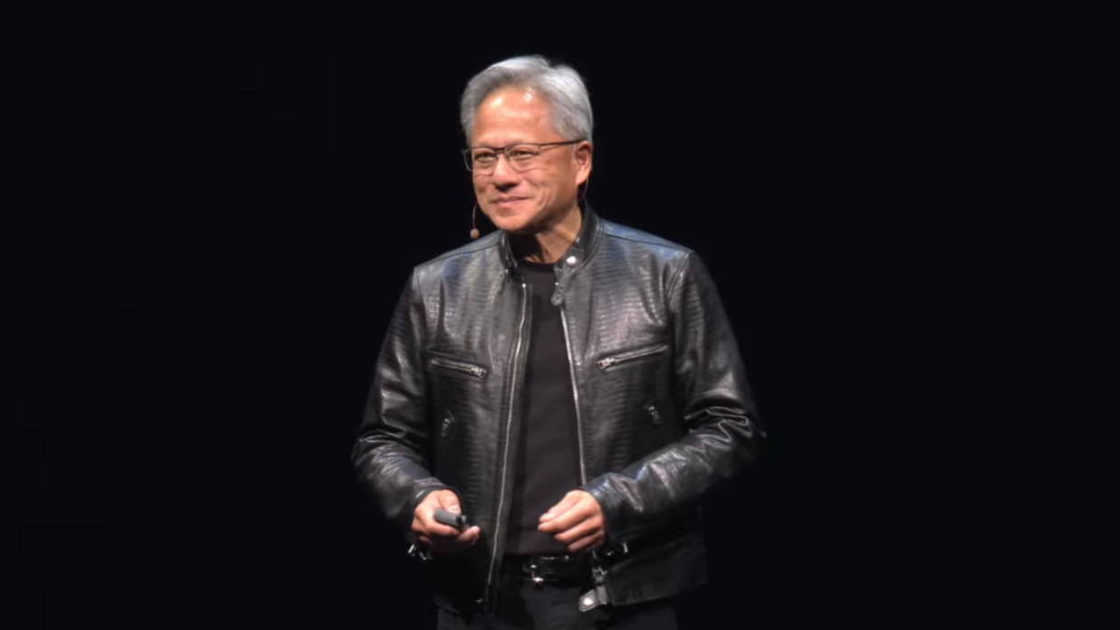
Nvidia CEO Jensen Huang has confirmed a design flaw in its top-end Blackwell AI chips which had affected production was an entirely internal problem, which has now been fixed.
"We had a design flaw in Blackwell," Huang said at an event in Copenhagen, Reuters reported. "It was functional, but the design flaw caused the yield to be low. It was 100% Nvidia's fault."
First identified in August 2024, the delay to Blackwell B100/B200 processors had raised eyebrows around the world, but Huang reassured that it was Nvidia's own doing that caused the issue.
Blackwell delays
Blackwell chips have been in high demand since Nvidia unveiled the platform earlier in 2024, with Huang describing it as, "the world's most powerful chip," offering previously unheard-of levels of AI computing power.
Set to begin shipping in the latter part of 2024, Blackwell binds together two GPU dies, which are connected by 10 TB/second chip-to-chip link into a single, unified GPU. This uses using TSMC's CoWoS-L packaging technology, which relies on an RDL interposer equipped with local silicon interconnect (LSI) bridges that need to be located specifically to allow fast data transfer - the misalignment of which resulted in the issue.
Initial media reports had claimed the issue had caused friction with manufacturing partner TSMC, but Huang dismissed the claims as "fake news".
"In order to make a Blackwell computer work, seven different types of chips were designed from scratch and had to be ramped into production at the same time," he said.
"What TSMC did, was to help us recover from that yield difficulty and resume the manufacturing of Blackwell at an incredible pace."
Blackwell is set to be up to 30x faster than its Grace Hopper predecessor when it comes to AI inference tasks, whilst also reducing cost and energy consumption by up to 25x.


